JAJSH18A March 2019 – September 2019 TPS7A78
PRODUCTION DATA.
- 1 特長
- 2 アプリケーション
- 3 概要
- 4 改訂履歴
- 5 概要(続き)
- 6 Pin Configuration and Functions
- 7 Specifications
-
8 Detailed Description
- 8.1 Overview
- 8.2 Functional Block Diagram
- 8.3
Feature Description
- 8.3.1 Active Bridge Control
- 8.3.2 Full-Bridge (FB) and Half-Bridge (HB) Configurations
- 8.3.3 4:1 Switched-Capacitor Voltage Reduction
- 8.3.4 Undervoltage Lockout Circuits (VUVLO_SCIN) and (VUVLO_LDO_IN)
- 8.3.5 Dropout Voltage Regulation
- 8.3.6 Current Limit
- 8.3.7 Programmable Power-Fail Detection
- 8.3.8 Power-Good (PG) Detection
- 8.3.9 Thermal Shutdown
- 8.4 Device Functional Modes
-
9 Application and Implementation
- 9.1
Application Information
- 9.1.1 Recommended Capacitor Types
- 9.1.2 Input and Output Capacitors Requirements
- 9.1.3 Startup Behavior
- 9.1.4 Load Transient
- 9.1.5 Standby Power and Output Efficiency
- 9.1.6 Reverse Current
- 9.1.7 Switched-Capacitor Stage Output Impedance
- 9.1.8 Power Dissipation (PD)
- 9.1.9 Estimating Junction Temperature
- 9.2
Typical Application
- 9.2.1 Design Requirements
- 9.2.2
Detailed Design Procedure
- 9.2.2.1 Calculating the Cap-Drop Capacitor CS
- 9.2.2.2 Calculating the Surge Resistor RS
- 9.2.2.3 Checking for the Device Maximum ISHUNT Current
- 9.2.2.4 Calculating the Bulk Capacitor CSCIN
- 9.2.2.5 Calculating the PFD Pin Resistor Dividers for a Power-Fail Detection
- 9.2.2.6 Summary of the Typical Application Design Components
- 9.2.3 Application Curves
- 9.1
Application Information
- 10Power Supply Recommendations
- 11Layout
- 12デバイスおよびドキュメントのサポート
- 13メカニカル、パッケージ、および注文情報
9.2 Typical Application
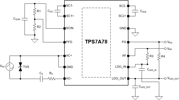
This section demonstrates the design process for a typical application of the TPS7A78, including the calculation of the values of the external components required for proper operation. Figure 33 shows an optimized electricity meter application using an HB configuration. For this design, the AC supply line voltage is referenced to the TPS7A78 GND pins to share the same GND as the system microcontroller.
 Figure 33. Example for a Single-Phase Electricity Meter Configuration