JAJSHU7D August   2019  – April 2021 THS6222

PRODUCTION DATA  

  1. 特長
  2. アプリケーション
  3. 概要
  4. Revision History
  5. Pin Configuration and Functions
  6. Specifications
    1. 6.1 Absolute Maximum Ratings
    2. 6.2 ESD Ratings
    3. 6.3 Recommended Operating Conditions
    4. 6.4 Thermal Information
    5. 6.5 Electrical Characteristics: VS = 12 V
    6. 6.6 Electrical Characteristics: VS = 32 V
    7. 6.7 Timing Requirements
    8. 6.8 Typical Characteristics: VS = 12 V
    9. 6.9 Typical Characteristics: VS = 32 V
  7. Detailed Description
    1. 7.1 Overview
    2. 7.2 Functional Block Diagram
    3. 7.3 Feature Description
      1. 7.3.1 Common-Mode Buffer
      2. 7.3.2 Thermal Protection and Package Power Dissipation
      3. 7.3.3 Output Voltage and Current Drive
      4. 7.3.4 Breakdown Supply Voltage
      5. 7.3.5 Surge Test Results
    4. 7.4 Device Functional Modes
  8. Application and Implementation
    1. 8.1 Application Information
    2. 8.2 Typical Applications
      1. 8.2.1 Broadband PLC Line Driving
        1. 8.2.1.1 Design Requirements
        2. 8.2.1.2 Detailed Design Procedure
        3. 8.2.1.3 Application Curve
    3. 8.3 What to Do and What Not to Do
      1. 8.3.1 Do
      2. 8.3.2 Do Not
  9. Power Supply Recommendations
  10. 10Layout
    1. 10.1 Layout Guidelines
    2. 10.2 Wafer and Die Information
    3. 10.3 Layout Examples
  11. 11Device and Documentation Support
    1. 11.1 Development Support
    2. 11.2 Documentation Support
      1. 11.2.1 Related Documentation
    3. 11.3 Receiving Notification of Documentation Updates
    4. 11.4 サポート・リソース
    5. 11.5 Trademarks
    6. 11.6 Electrostatic Discharge Caution
    7. 11.7 Glossary
  12. 12Mechanical, Packaging, and Orderable Information

Common-Mode Buffer

The THS6222 is a differential line driver that features an integrated common-mode buffer. Most common line driving applications for the THS6222 are ac-coupled applications; see Figure 8-2. Therefore, the inputs must be common-mode shifted to ensure the input signals are within the common-mode specifications of the device. To maximize the dynamic range, the common-mode voltage is shifted to midsupply in most ac-coupled applications. With the integrated common-mode buffer, no external components are required to shift the input common-mode voltage. Often, engineers choose to connect a noise-decoupling capacitor to the VCM pin. However, as shown in Figure 7-1, assuming the circuit is reasonably shielded from external noise sources, no difference in common-mode noise is observed with the 100 nF capacitor or without the capacitor.
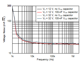
GUID-644B0AA1-8196-4113-BE1E-483E81B27F3A-low.gifFigure 7-1 Common-Mode Voltage Noise Density vs Frequency

There are ESD protection diodes in series directly at the output of the common-mode buffer between the internal 520 Ω resistor and the common-mode buffer output. These diodes are referenced to midsupply. Any voltage that is 1.4 V above or below the midsupply applied to the VCM pin forward biases the protection diodes. This biasing results in either current flowing into or out of the VCM pin. The current is limited by the 520 Ω resistor in series, but to prevent permanent damage to the device, the current must be limited to the current specifications in the Absolute Maximum Ratings table.