JAJSHW2A August 2019 – April 2020 DRV425-Q1
PRODUCTION DATA.
- 1 特長
- 2 アプリケーション
- 3 概要
- 4 改訂履歴
- 5 概要(続き)
- 6 Pin Configuration and Functions
- 7 Specifications
- 8 Detailed Description
- 9 Application and Implementation
- 10Power Supply Recommendations
- 11Layout
- 12デバイスおよびドキュメントのサポート
- 13メカニカル、パッケージ、および注文情報
8.3.2 Shunt-Sense Amplifier
The compensation coil current creates a voltage drop across the external shunt resistor, RSHUNT. The internal differential amplifier senses this voltage drop. This differential amplifier offers wide bandwidth and a high slew rate. Excellent dc stability and accuracy result from a chopping technique. The voltage gain is 4 V/V, set by precisely matched and thermally stable internal resistors.
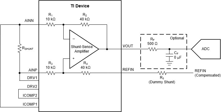
Both the AINN and AINP differential amplifier inputs are connected to the external shunt resistor. This shunt resistor, in series with the internal 10-kΩ input resistors of the shunt-sense amplifier, causes an additional gain error. Therefore, for best common-mode rejection performance, place a dummy shunt resistor (R5) with a value higher than the shunt resistor in series with the REFIN pin to restore the matching of both resistor dividers, as shown in Figure 65.
 Figure 65. Internal Difference Amplifier With an Example of a Decoupling Filter
 For an overall gain of 4 V/V, calculate the value of R5 using Equation 6:

where
- R2 / R1 = R4 / R3 = 4.
- R5 = RSHUNT × 4.
If the input signal is large, the amplifier output drives close to the supply rails. The amplifier output is able to drive the input of a successive approximation register (SAR) analog-to-digital converter (ADC). For best performance, add an RC low-pass filter stage between the shunt-sense amplifier output and the ADC input. This filter limits the noise bandwidth, and decouples the high-frequency sampling noise of the ADC input from the amplifier output. For filter resistor RF and filter capacitor CF values, see the specific converter recommendations in the respective product data sheet.
The shunt-sense amplifier output drives 100 pF directly, and shows a 50% overshoot with a 1-nF capacitance. Filter resistor RF extends the capacitive load range. With an RF of only 20 Ω, the load capacitor must be either less than 1 nF or more than 33 nF to avoid overshoot; with an RF of 50 Ω, this transient area is avoided.
Reference input REFIN is the common-mode voltage node for the output signal VOUT. To use the internal voltage reference of the DRV425-Q1, connect the REFIN pin to the reference output REFOUT. To avoid mismatch errors, use the same reference voltage for REFIN and the ADC. Alternatively, use an ADC with a pseudodifferential input, with the positive input of the ADC connected to VOUT, and the negative input connected to REFIN of the device.