JAJSHX4D November   2012  – September 2019 ADS1018

PRODUCTION DATA.  

  1. 特長
  2. アプリケーション
  3. 概要
    1.     Device Images
      1.      K タイプの熱電対測定 内蔵温度センサによる冷接点補償
  4. 改訂履歴
  5. 概要(続き)
  6. Device Comparison Table
  7. Pin Configuration and Functions
    1.     Pin Functions
  8. Specifications
    1. 8.1 Absolute Maximum Ratings
    2. 8.2 ESD Ratings
    3. 8.3 Recommended Operating Conditions
    4. 8.4 Thermal Information
    5. 8.5 Electrical Characteristics
    6. 8.6 Timing Requirements: Serial Interface
    7. 8.7 Switching Characteristics: Serial Interface
    8. 8.8 Typical Characteristics
  9. Detailed Description
    1. 9.1 Overview
    2. 9.2 Functional Block Diagram
    3. 9.3 Feature Description
      1. 9.3.1 Multiplexer
      2. 9.3.2 Analog Inputs
      3. 9.3.3 Full-Scale Range (FSR) and LSB Size
      4. 9.3.4 Voltage Reference
      5. 9.3.5 Oscillator
      6. 9.3.6 Temperature Sensor
        1. 9.3.6.1 Converting from Temperature to Digital Codes
        2. 9.3.6.2 Converting from Digital Codes to Temperature
    4. 9.4 Device Functional Modes
      1. 9.4.1 Reset and Power-Up
      2. 9.4.2 Operating Modes
        1. 9.4.2.1 Single-Shot Mode and Power-Down
        2. 9.4.2.2 Continuous-Conversion Mode
      3. 9.4.3 Duty Cycling for Low Power
    5. 9.5 Programming
      1. 9.5.1 Serial Interface
      2. 9.5.2 Chip Select (CS)
      3. 9.5.3 Serial Clock (SCLK)
      4. 9.5.4 Data Input (DIN)
      5. 9.5.5 Data Output and Data Ready (DOUT/DRDY)
      6. 9.5.6 Data Format
      7. 9.5.7 Data Retrieval
        1. 9.5.7.1 32-Bit Data Transmission Cycle
        2. 9.5.7.2 16-Bit Data Transmission Cycle
    6. 9.6 Register Maps
      1. 9.6.1 Conversion Register [reset = 0000h]
        1. Table 4. Conversion Register Field Descriptions
      2. 9.6.2 Config Register [reset = 058Bh]
        1. Table 5. Config Register Field Descriptions
  10. 10Application and Implementation
    1. 10.1 Application Information
      1. 10.1.1 Serial Interface Connections
      2. 10.1.2 GPIO Ports for Communication
      3. 10.1.3 Analog Input Filtering
      4. 10.1.4 Single-Ended Inputs
      5. 10.1.5 Connecting Multiple Devices
      6. 10.1.6 Pseudo Code Example
    2. 10.2 Typical Application
      1. 10.2.1 Design Requirements
      2. 10.2.2 Detailed Design Procedure
      3. 10.2.3 Application Curves
  11. 11Power Supply Recommendations
    1. 11.1 Power-Supply Sequencing
    2. 11.2 Power-Supply Decoupling
  12. 12Layout
    1. 12.1 Layout Guidelines
    2. 12.2 Layout Example
  13. 13デバイスおよびドキュメントのサポート
    1. 13.1 ドキュメントのサポート
      1. 13.1.1 関連資料
    2. 13.2 ドキュメントの更新通知を受け取る方法
    3. 13.3 コミュニティ・リソース
    4. 13.4 商標
    5. 13.5 静電気放電に関する注意事項
    6. 13.6 Glossary
  14. 14メカニカル、パッケージ、および注文情報

Connecting Multiple Devices

When connecting multiple ADS1018 devices to a single SPI bus, SCLK, DIN, and DOUT/DRDY can be safely shared by using a dedicated chip-select (CS) for each SPI-enabled device. By default, when CS goes high for the ADS1018, DOUT/DRDY is pulled up to VDD by a weak pullup resistor. This feature prevents DOUT/DRDY from floating near midrail and causing excess current leakage on a microcontroller input. If the PULL_UP_EN bit in the Config register is set to 0, the DOUT/DRDY pin enters a 3-state mode when CS transitions high. The ADS1018 cannot issue a data-ready pulse on DOUT/DRDY when CS is high. To evaluate when a new conversion is ready from the ADS1018 when using multiple devices, the master can periodically drop CS to the ADS1018. When CS goes low, the DOUT/DRDY pin immediately drives either high or low. If the DOUT/DRDY line drives low on a low CS, new data are currently available for clocking out at any time. If the DOUT/DRDY line drives high, no new data are available and the ADS1018 returns the last read conversion result. Valid data can be retrieved from the ADS1018 at anytime without concern of data corruption. If a new conversion becomes available during data transmission, that conversion is not available for readback until a new SPI transmission is initiated.
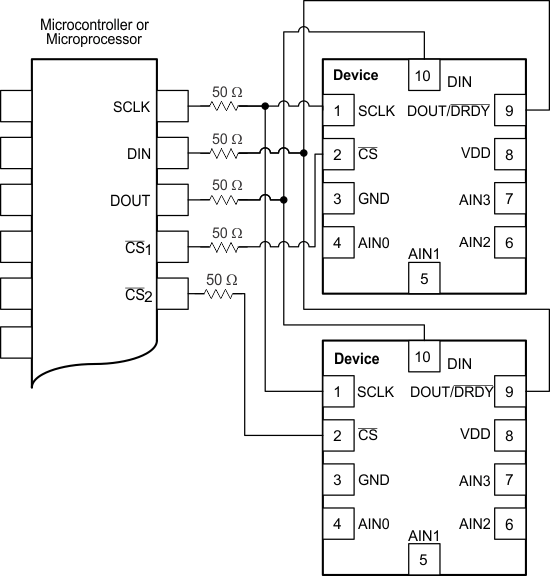
ADS1018 ai_mult_dev_bas457.gif
NOTE: Power and input connections omitted for clarity.
Figure 21. Connecting Multiple ADS1018s