JAJSI27A October   2019  – December 2019 DAC11001A , DAC81001 , DAC91001

UNLESS OTHERWISE NOTED, this document contains PRODUCTION DATA.  

  1. 特長
  2. アプリケーション
  3. 概要
    1.     Device Images
      1.      機能ブロック図
      2.      高精度の制御ループ回路
  4. 改訂履歴
  5. 概要(続き)
  6. Device Comparison Table
  7. Pin Configuration and Functions
    1.     Pin Functions
  8. Specifications
    1. 8.1      Absolute Maximum Ratings
    2. 8.2      ESD Ratings
    3. 8.3      Recommended Operating Conditions
    4. 8.4      Thermal Information Package
    5. 8.5      Electrical Characteristics
    6. Table 1. Timing Requirements: Write, 4.5 V ≤ DVDD ≤ 5.5 V
    7. Table 2. Timing Requirements: Write, 2.7 V ≤ DVDD < 4.5 V
    8. Table 3. Timing Requirements: Read and Daisy-Chain Write, 4.5 V ≤ DVDD ≤ 5.5 V
    9. Table 4. Timing Requirements: Read and Daisy-Chain Write, 2.7 V ≤ DVDD < 4.5 V
    10. 8.6      Typical Characteristics
  9. Detailed Description
    1. 9.1 Overview
    2. 9.2 Functional Block Diagram
    3. 9.3 Feature Description
      1. 9.3.1 Digital-to-Analog Converter Architecture
      2. 9.3.2 External Reference
      3. 9.3.3 Output Buffers
      4. 9.3.4 Internal Power-On Reset (POR)
      5. 9.3.5 Temperature Drift and Calibration
      6. 9.3.6 DAC Output Deglitch Circuit
    4. 9.4 Device Functional Modes
      1. 9.4.1 Fast-Settling Mode and THD
      2. 9.4.2 DAC Update Rate Mode
    5. 9.5 Programming
      1. 9.5.1 Daisy-Chain Operation
      2. 9.5.2 CLR Pin Functionality and Software Clear
      3. 9.5.3 Output Update (Synchronous and Asynchronous)
        1. 9.5.3.1 Synchronous Update
        2. 9.5.3.2 Asynchronous Update
      4. 9.5.4 Software Reset Mode
    6. 9.6 Register Map
      1. 9.6.1 NOP Register (address = 00h) [reset = 0x000000h]
        1. Table 9. NOP Register Field Descriptions
      2. 9.6.2 DAC-DATA Register (address = 01h) [reset = 0x000000h]
        1. Table 10. DAC-DATA Register Field Descriptions
      3. 9.6.3 CONFIG1 Register (address = 02h) [reset = 004C80h for bits [23:0]]
        1. Table 11. CONFIG1 Register Field Descriptions
      4. 9.6.4 DAC-CLEAR-DATA Register (address = 03h) [reset = 000000h for bits [23:0]]
        1. Table 12. DAC-CLEAR-DATA Register Field Descriptions
      5. 9.6.5 TRIGGER Register (address = 04h) [reset = 000000h for bits [23:0]]
        1. Table 13. TRIGGER Register Field Descriptions
      6. 9.6.6 STATUS Register (address = 05h) [reset = 000000h for bits [23:0]]
        1. Table 14. STATUS Register Field Descriptions
      7. 9.6.7 CONFIG2 Register (address = 06h) [reset = 000040h for bits [23:0]]
        1. Table 15. CONFIG2 Register Field Descriptions
  10. 10Application and Implementation
    1. 10.1 Application Information
    2. 10.2 Typical Application
      1. 10.2.1 Source Measure Unit (SMU)
        1. 10.2.1.1 Design Requirements
        2. 10.2.1.2 Detailed Design Procedure
        3. 10.2.1.3 Application Curves
      2. 10.2.2 Battery Test Equipment (BTE)
        1. 10.2.2.1 Design Requirements
        2. 10.2.2.2 Detailed Design Procedure
        3. 10.2.2.3 Application Curves
      3. 10.2.3 High-Precision Control Loop
        1. 10.2.3.1 Design Requirements
        2. 10.2.3.2 Detailed Design Procedure
        3. 10.2.3.3 Application Curves
      4. 10.2.4 Arbitrary Waveform Generation (AWG)
        1. 10.2.4.1 Design Requirements
        2. 10.2.4.2 Detailed Design Procedure
        3. 10.2.4.3 Application Curves
    3. 10.3 System Examples
      1. 10.3.1 Interfacing to a Processor
      2. 10.3.2 Interfacing to a Low-Jitter LDAC Source
      3. 10.3.3 Embedded Resistor Configurations
        1. 10.3.3.1 Minimizing Bias Current Mismatch
        2. 10.3.3.2 2x Gain configuration
        3. 10.3.3.3 Generating Negative Reference
    4. 10.4 What to Do and What Not to Do
      1. 10.4.1 What to Do
      2. 10.4.2 What Not to Do
    5. 10.5 Initialization Set Up
  11. 11Power Supply Recommendations
    1. 11.1 Power-Supply Sequencing
  12. 12Layout
    1. 12.1 Layout Guidelines
    2. 12.2 Layout Example
  13. 13デバイスおよびドキュメントのサポート
    1. 13.1 デバイス・サポート
      1. 13.1.1 開発サポート
    2. 13.2 ドキュメントのサポート
      1. 13.2.1 関連資料
    3. 13.3 関連リンク
    4. 13.4 ドキュメントの更新通知を受け取る方法
    5. 13.5 サポート・リソース
    6. 13.6 商標
    7. 13.7 静電気放電に関する注意事項
    8. 13.8 Glossary
  14. 14メカニカル、パッケージ、および注文情報

Typical Characteristics

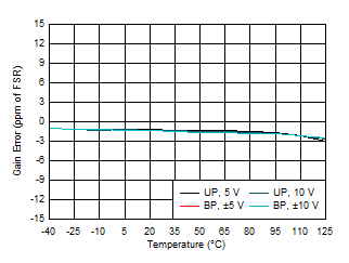
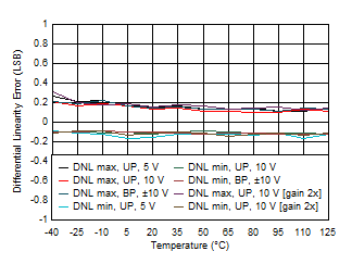
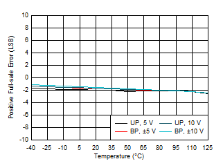
at TA = 25°C, VCC = 15 V, VSS = –15 V, AVDD = 5 V, IOVDD = 1.8 V, gain resistors unconnected (gain = 1x), OPA827 used as output and reference amplifier, UP = unipolar, BP = bipolar, and temperature calibration disabled (unless otherwise noted)
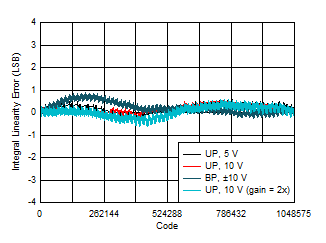
DAC11001A DAC91001 DAC81001 D001_SLASEL0.gif
Figure 3. . Integral Linearity Error vs Digital Input Code
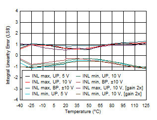
DAC11001A DAC91001 DAC81001 D003_SLASEL0.gif
Figure 5. Integral Linearity Error vs Temperature
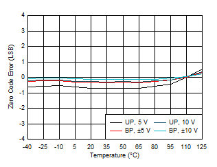
DAC11001A DAC91001 DAC81001 D005_SLASEL0.gif Figure 7. Zero Code Error vs Temperature
DAC11001A DAC91001 DAC81001 D009_SLASEL0.gif Figure 9. Gain Error vs Temperature
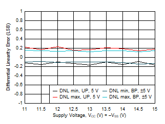
DAC11001A DAC91001 DAC81001 D011_SLASEL0.gif
Figure 11. Differential Linearity Error vs Supply Voltage
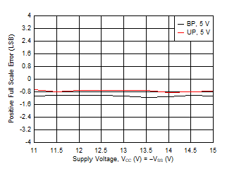
DAC11001A DAC91001 DAC81001 D013_SLASEL0.gif
Figure 13. Positive Full-Scale Error vs Supply Voltage
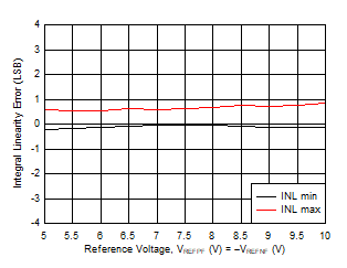
DAC11001A DAC91001 DAC81001 D016_SLASEL0.gif
Figure 15. Integral Linearity Error vs Reference Voltage
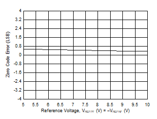
DAC11001A DAC91001 DAC81001 D018A_SLASEL0.gif
Figure 17. Zero Code Error vs Reference Voltage
DAC11001A DAC91001 DAC81001 D019_SLASEL0.gif
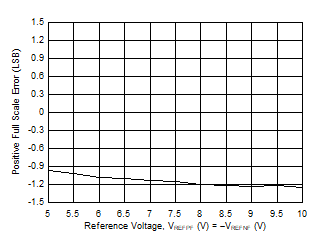
Figure 19. Positive Full-Scale Error vs Reference Voltage
DAC11001A DAC91001 DAC81001 D020A_SLASEL0.gif
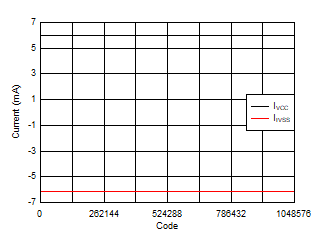
VREFPF = 10 V, VREFNF = 0 V
Figure 21. Supply Current (VCC and VSS)
vs Digital Input Code
DAC11001A DAC91001 DAC81001 D020C_SLASEL0.gif
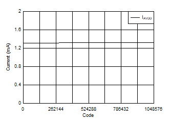
VREFPF = 10 V, VREFNF = 0 V
Figure 23. Supply Current (AVDD) vs Digital Input Code
DAC11001A DAC91001 DAC81001 D021B_SLASEL0.gif
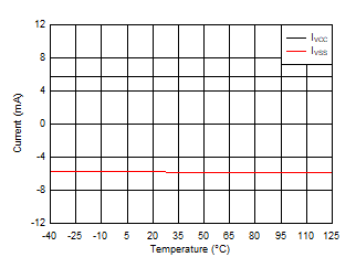
VREFPF = 10 V, VREFNF = 0 V, DAC at midcode
Figure 25. Supply Current (VCC and VSS)
vs Temperature
DAC11001A DAC91001 DAC81001 D021D_SLASEL0.gif
VREFPF = 10 V, VREFNF = 0 V, DAC at midcode
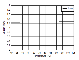
Figure 27. Supply Current (AVDD) vs Temperature
DAC11001A DAC91001 DAC81001 D023A_SLASEL0.gif
VREFPF = 10 V, VREFNF = 0 V, DAC at midcode
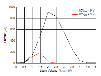
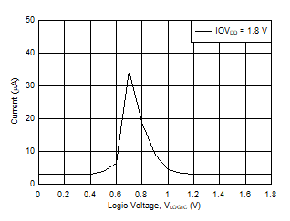
Figure 29. Supply Current (IOVDD)
vs Input Pin Logic Level
DAC11001A DAC91001 DAC81001 D024_SLASEL0.gif
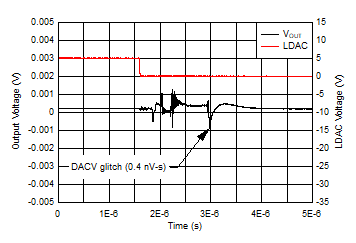
VREFPF = 10 V, VREFNF = –10 V, DAC transition midcode – 1 to midcode
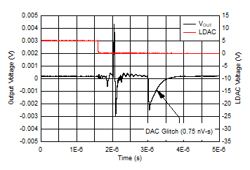
Figure 31. Glitch Impulse, Rising Edge, 1-LSB Step
DAC11001A DAC91001 DAC81001 D026_SLASEL0.gif
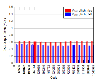
VREFPF = 10 V, VREFNF = –10 V
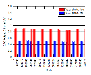
Figure 33. Segment Glitch Impulse, 1-LSB Step
DAC11001A DAC91001 DAC81001 D028_SLASEL0.gif
VREFPF = 5 V, VREFNF = 0 V
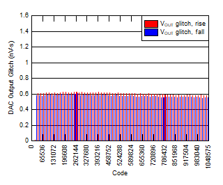
Figure 35. Segment Glitch Impulse, 1-LSB Step
DAC11001A DAC91001 DAC81001 D030_SLASEL0.gif
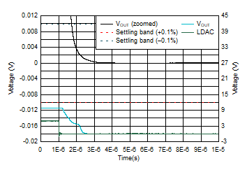
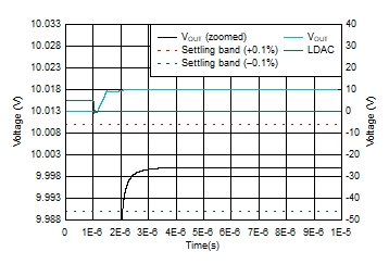
VREFPF = 10 V, VREFNF = 0 V
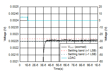
Figure 37. Full-Scale Settling Time, Falling Edge
DAC11001A DAC91001 DAC81001 D032_SLASEL0.gif
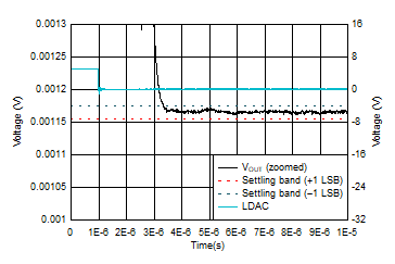
VREFPF = 10 V, VREFNF = 0 V, DAC transitions 100 codes around midscale
Figure 39. 100 Codes Settling Time, Falling Edge
DAC11001A DAC91001 DAC81001 D036_SLASEL0.gif
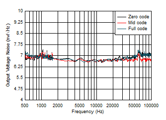
VREFPF = 10 V, VREFNF = 0 V, measured at DAC output
Figure 41. DAC Output Noise Spectral Density
DAC11001A DAC91001 DAC81001 D038_SLASEL0.gif
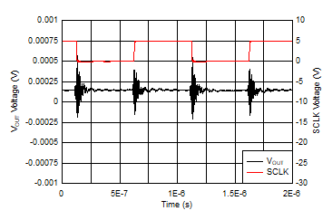
VREFPF = 10 V, VREFNF = 0 V, DAC at midcode, measured at DAC output pin
Figure 43. Clock Feedthrough
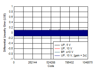
DAC11001A DAC91001 DAC81001 D002_SLASEL0.gif
Figure 4. Differential Linearity Error vs Digital Input Code
DAC11001A DAC91001 DAC81001 D004_SLASEL0.gif Figure 6. Differential Linearity Error vs Temperature
DAC11001A DAC91001 DAC81001 D008_SLASEL0.gif Figure 8. Positive Full-Scale Error vs Temperature
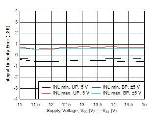
DAC11001A DAC91001 DAC81001 D010_SLASEL0.gif
Figure 10. Integral Linearity Error vs Supply Voltage
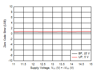
DAC11001A DAC91001 DAC81001 D012_SLASEL0.gif
Figure 12. Zero Code Error vs Supply Voltage
DAC11001A DAC91001 DAC81001 D014_SLASEL0.gif
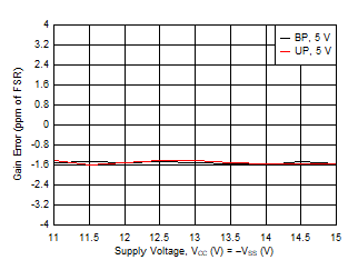
Figure 14. Gain Error vs Supply Voltage
DAC11001A DAC91001 DAC81001 D017_SLASEL0.gif
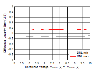
Figure 16. Differential Linearity Error vs Reference Voltage
DAC11001A DAC91001 DAC81001 D018_SLASEL0.gif
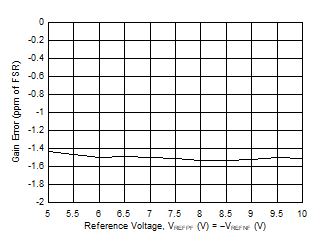
Figure 18. Gain Error vs Reference Voltage
DAC11001A DAC91001 DAC81001 D020_SLASEL0.gif
VREFPF = 10 V, VREFNF = 0 V
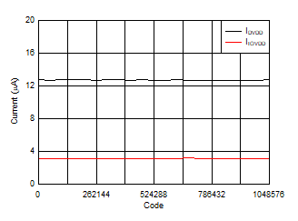
Figure 20. Supply Current (DVDD and IOVDD)
vs Digital Input Code
DAC11001A DAC91001 DAC81001 D020B_SLASEL0.gif
VREFPF = 10 V, VREFNF = 0 V
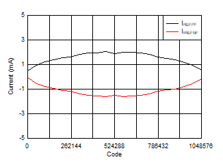
Figure 22. Reference Current (VREFPF and VREFNF)
vs Digital Input Code
DAC11001A DAC91001 DAC81001 D021A_SLASEL0.gif
VREFPF = 10 V, VREFNF = 0 V, DAC at midcode
Figure 24. Supply Current (DVDD) vs Temperature
DAC11001A DAC91001 DAC81001 D021C_SLASEL0.gif
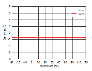
VREFPF = 10 V, VREFNF = 0 V, DAC at midcode
Figure 26. Reference Current (VREFPF and VREFNF)
vs Temperature
DAC11001A DAC91001 DAC81001 D022_SLASEL0.gif
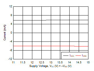
VREFPF = 5 V, VREFNF = 0 V, DAC at midcode
Figure 28. Supply Current (VCC and VSS) vs Supply Voltage
DAC11001A DAC91001 DAC81001 D023B_SLASEL0.gif
VREFPF = 10 V, VREFNF = 0 V, DAC at midcode
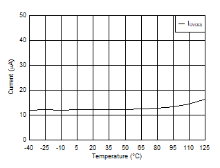
Figure 30. Supply Current (IOVDD = 1.8 V)
vs Input Pin Logic Level
DAC11001A DAC91001 DAC81001 D025_SLASEL0.gif
VREFPF = 10 V, VREFNF = –10 V, DAC transition midcode to midcode – 1
Figure 32. Glitch Impulse, Falling Edge, 1-LSB Step
DAC11001A DAC91001 DAC81001 D027_SLASEL0.gif
VREFPF = 10 V, VREFNF = 0 V
Figure 34. Segment Glitch Impulse, 1-LSB Step
DAC11001A DAC91001 DAC81001 D029_SLASEL0.gif
VREFPF = 10 V, VREFNF = 0 V
Figure 36. Full-Scale Settling Time, Rising Edge
DAC11001A DAC91001 DAC81001 D031_SLASEL0.gif
VREFPF = 10 V, VREFNF = 0 V, DAC transitions 100 codes around midscale
Figure 38. 100 Codes Settling Time, Rising Edge
DAC11001A DAC91001 DAC81001 D033_SLASEL0.gif
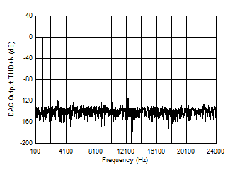
VREFPF = 10 V, VREFNF = 0 V, DAC output frequency = 1 kHz, DAC update rate = 400 kHz
Figure 40. Total Harmonic Distortion (THD + N)
vs Frequency
DAC11001A DAC91001 DAC81001 D037_SLASEL0.gif
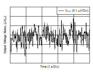
VREFPF = 10 V, VREFNF = 0 V, DAC at midcode, measured at DAC output pin
Figure 42. DAC Output Noise: 0.1 Hz to 10 Hz