JAJSI27A October   2019  – December 2019 DAC11001A , DAC81001 , DAC91001

UNLESS OTHERWISE NOTED, this document contains PRODUCTION DATA.  

  1. 特長
  2. アプリケーション
  3. 概要
    1.     Device Images
      1.      機能ブロック図
      2.      高精度の制御ループ回路
  4. 改訂履歴
  5. 概要(続き)
  6. Device Comparison Table
  7. Pin Configuration and Functions
    1.     Pin Functions
  8. Specifications
    1. 8.1      Absolute Maximum Ratings
    2. 8.2      ESD Ratings
    3. 8.3      Recommended Operating Conditions
    4. 8.4      Thermal Information Package
    5. 8.5      Electrical Characteristics
    6. Table 1. Timing Requirements: Write, 4.5 V ≤ DVDD ≤ 5.5 V
    7. Table 2. Timing Requirements: Write, 2.7 V ≤ DVDD < 4.5 V
    8. Table 3. Timing Requirements: Read and Daisy-Chain Write, 4.5 V ≤ DVDD ≤ 5.5 V
    9. Table 4. Timing Requirements: Read and Daisy-Chain Write, 2.7 V ≤ DVDD < 4.5 V
    10. 8.6      Typical Characteristics
  9. Detailed Description
    1. 9.1 Overview
    2. 9.2 Functional Block Diagram
    3. 9.3 Feature Description
      1. 9.3.1 Digital-to-Analog Converter Architecture
      2. 9.3.2 External Reference
      3. 9.3.3 Output Buffers
      4. 9.3.4 Internal Power-On Reset (POR)
      5. 9.3.5 Temperature Drift and Calibration
      6. 9.3.6 DAC Output Deglitch Circuit
    4. 9.4 Device Functional Modes
      1. 9.4.1 Fast-Settling Mode and THD
      2. 9.4.2 DAC Update Rate Mode
    5. 9.5 Programming
      1. 9.5.1 Daisy-Chain Operation
      2. 9.5.2 CLR Pin Functionality and Software Clear
      3. 9.5.3 Output Update (Synchronous and Asynchronous)
        1. 9.5.3.1 Synchronous Update
        2. 9.5.3.2 Asynchronous Update
      4. 9.5.4 Software Reset Mode
    6. 9.6 Register Map
      1. 9.6.1 NOP Register (address = 00h) [reset = 0x000000h]
        1. Table 9. NOP Register Field Descriptions
      2. 9.6.2 DAC-DATA Register (address = 01h) [reset = 0x000000h]
        1. Table 10. DAC-DATA Register Field Descriptions
      3. 9.6.3 CONFIG1 Register (address = 02h) [reset = 004C80h for bits [23:0]]
        1. Table 11. CONFIG1 Register Field Descriptions
      4. 9.6.4 DAC-CLEAR-DATA Register (address = 03h) [reset = 000000h for bits [23:0]]
        1. Table 12. DAC-CLEAR-DATA Register Field Descriptions
      5. 9.6.5 TRIGGER Register (address = 04h) [reset = 000000h for bits [23:0]]
        1. Table 13. TRIGGER Register Field Descriptions
      6. 9.6.6 STATUS Register (address = 05h) [reset = 000000h for bits [23:0]]
        1. Table 14. STATUS Register Field Descriptions
      7. 9.6.7 CONFIG2 Register (address = 06h) [reset = 000040h for bits [23:0]]
        1. Table 15. CONFIG2 Register Field Descriptions
  10. 10Application and Implementation
    1. 10.1 Application Information
    2. 10.2 Typical Application
      1. 10.2.1 Source Measure Unit (SMU)
        1. 10.2.1.1 Design Requirements
        2. 10.2.1.2 Detailed Design Procedure
        3. 10.2.1.3 Application Curves
      2. 10.2.2 Battery Test Equipment (BTE)
        1. 10.2.2.1 Design Requirements
        2. 10.2.2.2 Detailed Design Procedure
        3. 10.2.2.3 Application Curves
      3. 10.2.3 High-Precision Control Loop
        1. 10.2.3.1 Design Requirements
        2. 10.2.3.2 Detailed Design Procedure
        3. 10.2.3.3 Application Curves
      4. 10.2.4 Arbitrary Waveform Generation (AWG)
        1. 10.2.4.1 Design Requirements
        2. 10.2.4.2 Detailed Design Procedure
        3. 10.2.4.3 Application Curves
    3. 10.3 System Examples
      1. 10.3.1 Interfacing to a Processor
      2. 10.3.2 Interfacing to a Low-Jitter LDAC Source
      3. 10.3.3 Embedded Resistor Configurations
        1. 10.3.3.1 Minimizing Bias Current Mismatch
        2. 10.3.3.2 2x Gain configuration
        3. 10.3.3.3 Generating Negative Reference
    4. 10.4 What to Do and What Not to Do
      1. 10.4.1 What to Do
      2. 10.4.2 What Not to Do
    5. 10.5 Initialization Set Up
  11. 11Power Supply Recommendations
    1. 11.1 Power-Supply Sequencing
  12. 12Layout
    1. 12.1 Layout Guidelines
    2. 12.2 Layout Example
  13. 13デバイスおよびドキュメントのサポート
    1. 13.1 デバイス・サポート
      1. 13.1.1 開発サポート
    2. 13.2 ドキュメントのサポート
      1. 13.2.1 関連資料
    3. 13.3 関連リンク
    4. 13.4 ドキュメントの更新通知を受け取る方法
    5. 13.5 サポート・リソース
    6. 13.6 商標
    7. 13.7 静電気放電に関する注意事項
    8. 13.8 Glossary
  14. 14メカニカル、パッケージ、および注文情報

Application Curves

The test conditions for the THD values in the graph of Figure 66 are a ±3-V reference input on the BP-DAC11001EVM, and an external 3x gain at the DAC output. The THD calculation considers 11 harmonics; the even harmonics are omitted. When two DACs are used in a differential output mode, the even harmonics are cancelled to a large extent. Figure 66 shows an ideal scenario, when the even harmonics are completely cancelled out.
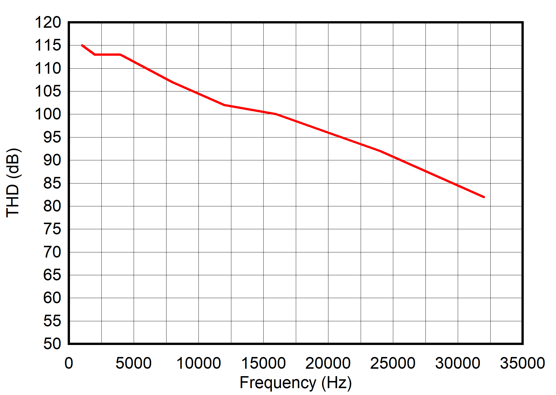
DAC11001A DAC91001 DAC81001 thd-measured-on-evm.pngFigure 66. THD vs Frequency