JAJSIJ6F April 2011 – February 2020 AMC1204
PRODUCTION DATA.
- 1 特長
- 2 アプリケーション
- 3 概要
- 4 改訂履歴
- 5 概要(続き)
- 6 Pin Configuration and Functions
-
7 Specifications
- 7.1 Absolute Maximum Ratings
- 7.2 ESD Ratings
- 7.3 Recommended Operating Conditions
- 7.4 Thermal Information
- 7.5 Power Ratings
- 7.6 Insulation Specifications
- 7.7 Safety-Related Certifications
- 7.8 Safety Limiting Values
- 7.9 Electrical Characteristics
- 7.10 Timing Requirements
- 7.11 Insulation Characteristics Curves
- 7.12 Typical Characteristics
- 8 Detailed Description
- 9 Application and Implementation
- 10Power Supply Recommendations
- 11Layout
- 12デバイスおよびドキュメントのサポート
- 13メカニカル、パッケージ、および注文情報
10 Power Supply Recommendations
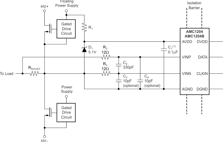
In a typical frequency inverter application, the high-side power supply (AVDD) for the AMC1204 and AMC1204B is derived from the power supply of the upper gate driver. For lowest cost, a Zener diode can be used to limit the voltage to 5 V ±10%. TI recommends a decoupling capacitor of 0.1 µF for filtering this power-supply path. This capacitor (C1 in Figure 55) should be placed as close as possible to the AVDD pin for best performance. If better filtering is required, an additional 1-µF to 10-µF capacitor can be used. The floating ground reference AGND is derived from the end of the shunt resistor, which is connected to the negative input (VINN) of the AMC1204 and AMC1204B. If a four-terminal shunt is used, the inputs of AMC1204 and AMC1204B are connected to the inner leads, while AGND is connected to one of the outer leads of the shunt. Both digital signals, CLKIN and DATA, can be directly connected to a digital filter.
For better performance, the differential input signal is filtered using RC filters (components R2, R3, and C2). Optionally, C3 and C4 can be used to reduce charge dumping from the inputs. In this case, care should be taken when choosing the quality of these capacitors: any mismatch in the capacitor values can cause a common-mode error at the input of the modulator.
