JAJSJ15B October 2020 – March 2022 TPS25947
PRODUCTION DATA
- 1 特長
- 2 アプリケーション
- 3 概要
- 4 Revision History
- 5 Device Comparison Table
- 6 Pin Configuration and Functions
- 7 Specifications
-
8 Detailed Description
- 8.1 Overview
- 8.2 Functional Block Diagram
- 8.3
Feature Description
- 8.3.1 Input Reverse Polarity Protection
- 8.3.2 Undervoltage Lockout (UVLO and UVP)
- 8.3.3 Overvoltage Lockout (OVLO)
- 8.3.4 Overvoltage Clamp (OVC)
- 8.3.5 Inrush Current, Overcurrent, and Short Circuit Protection
- 8.3.6 Analog Load Current Monitor
- 8.3.7 Reverse Current Protection
- 8.3.8 Overtemperature Protection (OTP)
- 8.3.9 Fault Response and Indication (FLT)
- 8.3.10 Auxiliary Channel Control (AUXOFF)
- 8.3.11 Power Good Indication (PG)
- 8.4 Device Functional Modes
- 9 Application and Implementation
- 10Power Supply Recommendations
- 11Layout
- 12Device and Documentation Support
- 13Mechanical, Packaging, and Orderable Information
9.4 Active ORing
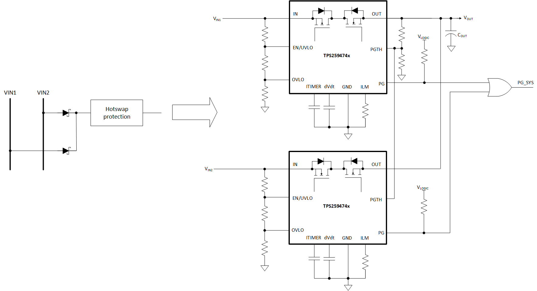
A typical redundant power supply configuration is shown in Figure 9-7 below. Schottky ORing diodes have been popular for connecting parallel power supplies, such as parallel operation of wall adapter with a battery or a hold-up storage capacitor. The disadvantage of using ORing diodes is high voltage drop and associated power loss. The TPS259470x/4x with integrated, low-ohmic, back-to-back FETs provide a simple and efficient solution. Figure 9-7 below shows the Active ORing implementation using TPS249474x devices.
 Figure 9-7 Two Devices, Active ORing
Configuration
Figure 9-7 Two Devices, Active ORing
ConfigurationThe linear ORing mechanism in TPS25947xx ensures that there's no reverse current flowing from one power source to the other during fast or slow ramp of either supply.
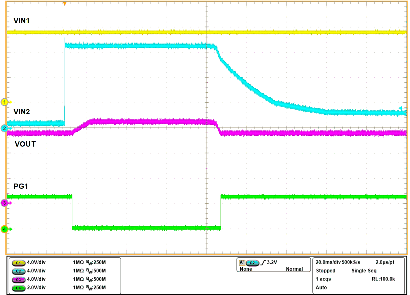
The following waveform illustrates the active ORing behavior when the supply rails are being ramped up sequentially.
 Figure 9-8 Active ORing Response
 Figure 9-9 Active ORing Response
When the bus voltages (IN1 and IN2) are matched, device in each path sees a forward voltage drop and is ON delivering the load current. During this period, current is shared between the rails in the ratio of differential voltage drop across each device.
In addition to supply ORing, the devices protect the system from overvoltage, excessive inrush current, overload and short-circuit faults at all times.
- The TPS259472x (OVC variants) are not recommended for use in ORing applications. While the device is in clamping state, if the output is forced to a higher voltage by the other channel, the device can get damaged.
- ORing can be done either between two similar rails or between dissimilar rails. For ORing cases with skewed voltage combinations, care must be taken to design circuit components on PGTH/EN/OVLO pins for the lower voltage channel devices such that the Absolute maximum ratings on those pins are not exceeded when higher voltage is present on the other channel. Also, the dVdt pin capacitor rating must be chosen based on the highest of the 2 supplies. Refer to Recommended Operating Conditions table for more details.