JAJSJ53B may 2020 – april 2023 TPD3S713-Q1 , TPD3S713A-Q1
PRODUCTION DATA
- 1
- 1 特長
- 2 アプリケーション
- 3 概要
- 4 Revision History
- 5 Pin Configuration and Functions
- 6 Specifications
- 7 Parameter Measurement Information
- 8 Detailed Description
- 9 Application and Implementation
- 10Device and Documentation Support
- 11Mechanical, Packaging, and Orderable Information
5 Pin Configuration and Functions
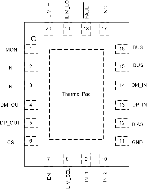
 Figure 5-1 RVC Package20-Pin WQFNTop View
Table 5-1 Pin Functions
| PIN | TYPE(1) | DESCRIPTION | |
|---|---|---|---|
| NAME | NO. | ||
| IMON | 1 | O | This pin sources a scaled-down ratio of current through the internal FET. A resistor from this pin to GND converts current to proportional voltage; used as an analog current monitor. |
| IN | 2,3 | PWR | Input supply voltage; connect a 0.1-µF or greater ceramic capacitor from IN to GND as close to the IC as possible. |
| DM_OUT | 4 | I/O | DM data line to upstream USB host controller |
| DP_OUT | 5 | I/O | DP data line to upstream USB host controller |
| CS | 6 | O | Linear cable compensation current. Connect to divider resistor of front-end dc-dc converter. |
| EN | 7 | I | Logic-level control input for turning the power and signal switches on or off. When EN is low, the device is disabled, and the signal and power switches are OFF. |
| ILIM_SEL | 8 | I | Logic-level control input for choosing the current limit resistor and current limit threshold. When ILIM_SEL = High, ILIM_HI resistor is valid; When ILIM_SEL = Low, ILIM_LO resistor is valid. |
| INT1 | 9 | I | Logic-level control input, the device can be set in normal mode or client mode through pin configuration. If INT1 = high, the device is in normal mode; If INT1 = low and ILIM_SEL = Low, the device is in client mode. |
| INT2 | 10 | I | For internal circuit, must connect to ground without a pull down resistor. |
| GND | 11 | — | Ground connection; must be connected externally to the thermal pad. |
| BIAS | 12 | PWR | Used for IEC protection. Typically, connect a 2.2-µF capacitor to ground and 5.1-kΩ resistor to BUS. |
| DP_IN | 13 | I/O | DP data line to downstream connector |
| DM_IN | 14 | I/O | DM data line to downstream connector |
| BUS | 15,16 | PWR | Power-switch output |
| NC | 17 | NC | No connect, leave floating or connect to ground. |
| FAULT | 18 | O | Active-low, open-drain output, asserted during overtemperature, overcurrent, and overvoltage conditions. |
| ILIM_LO | 19 | I | External resistor used to set the low current-limit threshold, selected by ILIM_SEL pin. |
| ILIM_HI | 20 | I | External resistor used to set the high current-limit threshold, selected by ILIM_SEL pin. |
| Thermal pad | — | Thermal pad on the bottom of the package | |
(1) I = Input, O = Output, I/O = Input and output, PWR = Power