JAJSJC1 September 2020 LM34966-Q1
PRODUCTION DATA
- 1 特長
- 2 アプリケーション
- 3 概要
- 4 Revision History
- 5 概要 (続き)
- 6 Pin Configuration and Functions
- 7 Specifications
-
8 Detailed Description
- 8.1 Overview
- 8.2 Functional Block Diagram
- 8.3
Feature Description
- 8.3.1 Line Undervoltage Lockout (UVLO/SYNC/EN Pin)
- 8.3.2 High Voltage VCC Regulator (BIAS, VCC Pin)
- 8.3.3 Soft Start (SS Pin)
- 8.3.4 Switching Frequency (RT Pin)
- 8.3.5 Clock Synchronization (UVLO/SYNC/EN Pin)
- 8.3.6 Current Sense and Slope Compensation (CS Pin)
- 8.3.7 Current Limit and Minimum On-time (CS Pin)
- 8.3.8 Feedback and Error Amplifier (FB, COMP Pin)
- 8.3.9 Power-Good Indicator (PGOOD Pin)
- 8.3.10 Hiccup Mode Overload Protection
- 8.3.11 Maximum Duty Cycle Limit and Minimum Input Supply Voltage
- 8.3.12 MOSFET Driver (GATE Pin)
- 8.3.13 Overvoltage Protection (OVP)
- 8.3.14 Thermal Shutdown (TSD)
- 8.4 Device Functional Modes
- 9 Application and Implementation
- 10Power Supply Recommendations
- 11Layout
- 12Device and Documentation Support
- 13Mechanical, Packaging, and Orderable Information
8.3.2 High Voltage VCC Regulator (BIAS, VCC Pin)
The device has an internal wide input VCC regulator which is sourced from the BIAS pin. The wide input VCC regulator allows the BIAS pin to be connected directly to supply voltages from 3.5 V to 40 V.
The VCC regulator turns on when the device is in standby or run mode. When the BIAS pin voltage is below the VCC regulation target, the VCC output tracks the BIAS with a small dropout voltage. When the BIAS pin voltage is greater than the VCC regulation target, the VCC regulator provides 6.85-V supply for the N-channel MOSFET driver.
The VCC regulator sources current into the capacitor connected to the VCC pin with a minimum of 35-mA capability. The recommended VCC capacitor value is from 1 µF to 4.7 µF.
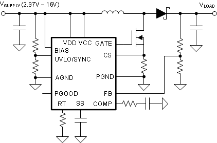
The device supports a wide input range from 3.5 V to 40 V in normal configuration. By connecting the BIAS pin directly to the VCC pin, the device supports inputs from 2.97 V to 16 V. This configuration is recommended when the device starts up from a 1-cell battery.
 Figure 8-5 2.97-V Start-Up
(BIAS = VCC)
Figure 8-5 2.97-V Start-Up
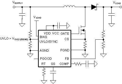
(BIAS = VCC)The minimum supply voltage after start-up can be further decreased by supplying the BIAS pin from the boost converter output or from an external power supply as shown in Figure 8-6.
 Figure 8-6 Decrease the Minimum Operating Voltage
After Start-Up
Figure 8-6 Decrease the Minimum Operating Voltage
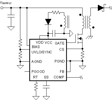
After Start-UpIn flyback topology, the internal power dissipation of the device can be decreased by supplying the VCC using an additional transformer winding. In this configuration, the external VCC supply voltage must be greater than the VCC regulation target (VVCC-REG), and the BIAS pin voltage must be greater the VCC voltage because the VCC regulator includes a diode between VCC and BIAS.
 Figure 8-7 External VCC Supply (BIAS ≥
VCC)
Figure 8-7 External VCC Supply (BIAS ≥
VCC)If the voltage of the external VCC bias supply is greater than the BIAS pin voltage, use an external blocking diode from the input power supply to the BIAS pin to prevent the external bias supply from passing current to the boost input supply through VCC.