JAJSJD6A July 2021 – December 2021 TPS22992
PRODUCTION DATA
- 1 特長
- 2 アプリケーション
- 3 概要
- 4 Revision History
- 5 Device Comparison Table
- 6 Pin Configuration and Functions
-
7 Specifications
- 7.1 Absolute Maximum Ratings
- 7.2 ESD Ratings
- 7.3 Recommended Operating Conditions
- 7.4 Thermal Information
- 7.5 Electrical Characteristics (VBIAS = 5 V)
- 7.6 Electrical Characteristics (VBIAS = 3.3 V)
- 7.7 Electrical Characteristics (VBIAS = 1.5 V)
- 7.8 Switching Characteristics (VBIAS = 5 V)
- 7.9 Switching Characteristics (VBIAS = 3.3 V)
- 7.10 Switching Characteristics (VBIAS = 1.5 V)
- 7.11 Typical Characteristics
- 8 Timing Diagram
- 9 Detailed Description
- 10Application and Implementation
- 11Power Supply Recommendations
- 12Layout
- 13Device and Documentation Support
- 14Mechanical, Packaging, and Orderable Information
6 Pin Configuration and Functions
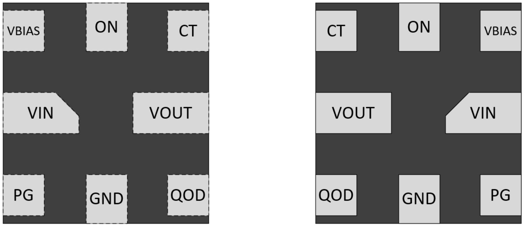
 Figure 6-1 TPS22992x Pinout (Top View Left, Bottom View Right)
Table 6-1 Pin Functions
| PIN | I/O(1) | DESCRIPTION | |
|---|---|---|---|
| NAME | NO. | ||
VBIAS | 1 | I | Bias voltage |
VIN | 2 | I | Input voltage |
PG | 3 | O | Open drain power good signal, asserted high when the output is full load ready |
GND | 4 | — | Device ground |
QOD | 5 | — | Quick output discharge pin |
VOUT | 6 | O | Output voltage |
CT | 7 | O | Timing pin, can control the slew rate of the output through a capacitor to GND |
ON | 8 | I | Enable pin |
(1) I = Input, O = Output, I/O = Input or Output, G = Ground, P = Power.