JAJSJH8A October 2020 – May 2021 DAC61402 , DAC81402
PRODUCTION DATA
- 1 特長
- 2 アプリケーション
- 3 概要
- 4 Revision History
- 5 Device Comparison Table
- 6 Pin Configuration and Functions
-
7 Specifications
- 7.1 Absolute Maximum Ratings
- 7.2 ESD Ratings
- 7.3 Recommended Operating Conditions
- 7.4 Thermal Information
- 7.5 Electrical Characteristics
- 7.6 Timing Requirements: Write, IOVDD: 1.7 V to 2.7 V
- 7.7 Timing Requirements: Write, IOVDD: 2.7 V to 5.5 V
- 7.8 Timing Requirements: Read and Daisy Chain, FSDO = 0, IOVDD: 1.7 V to 2.7 V
- 7.9 Timing Requirements: Read and Daisy Chain, FSDO = 1, IOVDD: 1.7 V to 2.7 V
- 7.10 Timing Requirements: Read and Daisy Chain, FSDO = 0, IOVDD: 2.7 V to 5.5 V
- 7.11 Timing Requirements: Read and Daisy Chain, FSDO = 1, IOVDD: 2.7 V to 5.5 V
- 7.12 Timing Diagrams
- 7.13 Typical Characteristics
-
8 Detailed Description
- 8.1 Overview
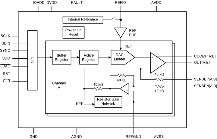
- 8.2 Functional Block Diagram
- 8.3 Feature Description
- 8.4 Device Functional Modes
- 8.5 Programming
- 8.6
Register Map
- 8.6.1 NOP Register (address = 00h) [reset = 0000h]
- 8.6.2 DEVICEID Register (address = 01h) [reset = 0A70h or 0930h]
- 8.6.3 STATUS Register (address = 02h) [reset = 0000h]
- 8.6.4 SPICONFIG Register (address = 03h) [reset = 0AA4h]
- 8.6.5 GENCONFIG Register (address = 04h) [reset = 4000h]
- 8.6.6 BRDCONFIG Register (address = 05h) [reset = 000Fh]
- 8.6.7 SYNCCONFIG Register (address = 06h) [reset = 0000h]
- 8.6.8 DACPWDWN Register (address = 09h) [reset = FFFFh]
- 8.6.9 DACRANGE Register (address = 0Ah) [reset = 0000h]
- 8.6.10 TRIGGER Register (address = 0Eh) [reset = 0000h]
- 8.6.11 BRDCAST Register (address = 0Fh) [reset = 0000h]
- 8.6.12 DACn Register (address = 11h to 12h) [reset = 0000h]
- 9 Application and Implementation
- 10Power Supply Recommendations
- 11Layout
- 12Device and Documentation Support
- 13Mechanical, Packaging, and Orderable Information
