JAJSJT6A August   2020  – July 2021 TPS65994AD

PRODUCTION DATA  

  1. 特長
  2. アプリケーション
  3. 概要
  4. Revision History
  5. Pin Configuration and Functions
  6. Specifications
    1. 6.1  Absolute Maximum Ratings
    2. 6.2  ESD Ratings
    3. 6.3  Recommended Operating Conditions
    4. 6.4  Recommended Capacitance
    5. 6.5  Thermal Information
    6. 6.6  Power Supply Characteristics
    7. 6.7  Power Consumption
    8. 6.8  PP_5V Power Switch Characteristics
    9. 6.9  PP_EXT Power Switch Characteristics
    10. 6.10 Power Path Supervisory
    11. 6.11 CC Cable Detection Parameters
    12. 6.12 CC VCONN Parameters
    13. 6.13 CC PHY Parameters
    14. 6.14 Thermal Shutdown Characteristics
    15. 6.15 ADC Characteristics
    16. 6.16 Input/Output (I/O) Characteristics
    17. 6.17 I2C Requirements and Characteristics
    18. 6.18 Typical Characteristics
  7. Parameter Measurement Information
  8. Detailed Description
    1. 8.1 Overview
    2. 8.2 Functional Block Diagram
    3. 8.3 Feature Description
      1. 8.3.1  USB-PD Physical Layer
        1. 8.3.1.1 USB-PD Encoding and Signaling
        2. 8.3.1.2 USB-PD Bi-Phase Marked Coding
        3. 8.3.1.3 USB-PD Transmit (TX) and Receive (Rx) Masks
        4. 8.3.1.4 USB-PD BMC Transmitter
        5. 8.3.1.5 USB-PD BMC Receiver
        6. 8.3.1.6 Squelch Receiver
      2. 8.3.2  Power Management
        1. 8.3.2.1 Power-On And Supervisory Functions
        2. 8.3.2.2 VBUS LDO
      3. 8.3.3  Power Paths
        1. 8.3.3.1 Internal Sourcing Power Paths
          1. 8.3.3.1.1  PP_5Vx Current Clamping
          2. 8.3.3.1.2  PP_5Vx Local Overtemperature Shut Down (OTSD)
          3. 8.3.3.1.3  PP_5Vx Current Sense
          4. 8.3.3.1.4  PP_5Vx OVP
          5. 8.3.3.1.5  PP_5Vx UVLO
          6. 8.3.3.1.6  PP_5Vx Reverse Current Protection
          7. 8.3.3.1.7  Fast Role Swap
          8. 8.3.3.1.8  PP_CABLE Current Clamp
          9. 8.3.3.1.9  PP_CABLE Local Overtemperature Shut Down (OTSD)
          10. 8.3.3.1.10 PP_CABLE UVLO
        2. 8.3.3.2 Sink Path Control
          1. 8.3.3.2.1 Overvoltage Protection (OVP)
          2. 8.3.3.2.2 Reverse-Current Protection (RCP)
          3. 8.3.3.2.3 VBUS UVLO
          4. 8.3.3.2.4 Discharging VBUS to Safe Voltage
      4. 8.3.4  Cable Plug and Orientation Detection
        1. 8.3.4.1 Configured as a Source
        2. 8.3.4.2 Configured as a Sink
        3. 8.3.4.3 Configured as a DRP
        4. 8.3.4.4 Fast Role Swap Signal Detection
        5. 8.3.4.5 Dead Battery Advertisement
      5. 8.3.5  Default Behavior Configuration (ADCIN1, ADCIN2)
      6. 8.3.6  ADC
      7. 8.3.7  DisplayPort Hot-Plug Detect (HPD)
      8. 8.3.8  Digital Interfaces
        1. 8.3.8.1 General GPIO
        2. 8.3.8.2 I2C Interface
      9. 8.3.9  Digital Core
      10. 8.3.10 I2C Interface
        1. 8.3.10.1 I2C Interface Description
        2. 8.3.10.2 I2C Clock Stretching
        3. 8.3.10.3 I2C Address Setting
        4. 8.3.10.4 Unique Address Interface
    4. 8.4 Device Functional Modes
      1. 8.4.1 Pin Strapping to Configure Default Behavior
      2. 8.4.2 Power States
      3. 8.4.3 Thermal Shutdown
  9. Application and Implementation
    1. 9.1 Application Information
    2. 9.2 Typical Application
      1. 9.2.1 Type-C VBUS Design Considerations
        1. 9.2.1.1 Design Requirements
        2. 9.2.1.2 Detailed Design Procedure
          1. 9.2.1.2.1 Type-C Connector VBUS Capacitors
          2. 9.2.1.2.2 VBUS Schottky and TVS Diodes
        3. 9.2.1.3 Application Curves
      2. 9.2.2 Notebook Design Supporting PD Charging
        1. 9.2.2.1 USB and DisplayPort Notebook Supporting PD Charging
          1. 9.2.2.1.1 Design Requirements
          2. 9.2.2.1.2 Detailed Design Procedure
            1. 9.2.2.1.2.1 USB Power Delivery Source Capabilities
            2. 9.2.2.1.2.2 USB Power Delivery Sink Capabilities
            3. 9.2.2.1.2.3 USB and DisplayPort Supported Data Modes
            4. 9.2.2.1.2.4 TUSB1046 Super Speed Mux GPIO Control
        2. 9.2.2.2 Thunderbolt Notebook Supporting PD Charging
          1. 9.2.2.2.1 Design Requirements
          2. 9.2.2.2.2 Detailed Design Procedure
            1. 9.2.2.2.2.1 USB Power Delivery Source Capabilities
            2. 9.2.2.2.2.2 USB Power Delivery Sink Capabilities
            3. 9.2.2.2.2.3 Thunderbolt Supported Data Modes
            4. 9.2.2.2.2.4 I2C Design Requirements
            5. 9.2.2.2.2.5 TS3DS10224 SBU Mux for AUX and LSTX/RX
  10. 10Power Supply Recommendations
    1. 10.1 3.3-V Power
      1. 10.1.1 VIN_3V3 Input Switch
      2. 10.1.2 VBUS 3.3-V LDO
    2. 10.2 1.5-V Power
    3. 10.3 Recommended Supply Load Capacitance
  11. 11Layout
    1. 11.1 Layout Guidelines
      1. 11.1.1 Top TPS65994AD Placement and Bottom Component Placement and Layout
    2. 11.2 Layout Example
    3. 11.3 Component Placement
    4. 11.4 Routing PP_5V, VBUS, VIN_3V3, LDO_3V3, LDO_1V5
    5. 11.5 Routing CC and GPIO
  12. 12Device and Documentation Support
    1. 12.1 Device Support
      1. 12.1.1 Third-Party Products Disclaimer
    2. 12.2 Documentation Support
      1. 12.2.1 Related Documentation
    3. 12.3 サポート・リソース
    4. 12.4 Trademarks
    5. 12.5 Electrostatic Discharge Caution
    6. 12.6 Glossary
  13. 13Mechanical, Packaging, and Orderable Information
    1. 13.1 Package Option Addendum
      1. 13.1.1 Tape and Reel Information

Default Behavior Configuration (ADCIN1, ADCIN2)

Note:

This functionality is firmware controlled and subject to change.

The ADCINx inputs to the internal ADC control the behavior of the TPS65994AD in response to PA_VBUS or PB_VBUS being supplied when VIN_3V3 is low (that is the dead-battery scenario). The ADCINx pins must be externally tied to the LDO_3V3 pin via a resistive divider as shown in the following figure. At power-up the ADC converts the ADCINx voltage and the digital core uses these two values to determine start-up behavior. The available start-up configurations include options for I2C slave address of I2C_EC_SCL/SDA, sink path control in dead-battery, and default configuration.
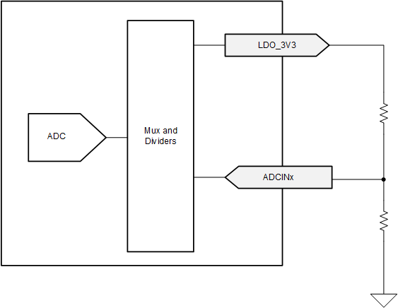
GUID-C0AFFF3F-03C9-48FF-8B24-8AFB9F0CC599-low.gif Figure 8-17 ADCINx Resistor Divider

The device behavior is determined in several ways depending upon the decoded value of the ADCIN1 and ADCIN2 pins. The following table shows the decoded values for different resistor divider ratios. See Pin Strapping to Configure Default Behavior for details on how the ADCINx configurations determine default device behavior. See I2C Address Setting for details on how ADCINx decoded values affects default I2C slave address.

Table 8-2 Decoding of ADCIN1 and ADCIN2 Pins
DIV = RDOWN / (RUP + RDOWN)(1) Without using RUP or RDOWN ADCINx decoded value
MIN Target MAX
0 0.0114 0.0228 tie to GND 0
0.0229 0.0475 0.0722 N/A 1
0.0723 0.1074 0.1425 N/A 2
0.1425 0.1899 0.2372 N/A 3
0.2373 0.3022 0.3671 N/A 4
0.3672 0.5368 0.7064 tie to LDO_1V5 5
0.7065 0.8062 0.9060 N/A 6
0.9061 0.9530 1.0 tie to LDO_3V3 7
External resistor tolerance of 1% is recommended. Resistor values must be chosen to yield a DIV value centered nominally between listed MIN and MAX values. For convenience, the Target column shows this value.