JAJSJT9A October 2020 – December 2020 LM7310
PRODUCTION DATA
- 1 特長
- 2 アプリケーション
- 3 概要
- 4 Revision History
- 5 Pin Configuration and Functions
- 6 Specifications
-
7 Detailed Description
- 7.1 Overview
- 7.2 Functional Block Diagram
- 7.3
Feature Description
- 7.3.1 Input Reverse Polarity Protection
- 7.3.2 Undervoltage Protection (UVLO & UVP)
- 7.3.3 Overvoltage Lockout (OVLO)
- 7.3.4 Inrush Current control and Fast-trip
- 7.3.5 Analog Load Current Monitor Output
- 7.3.6 Reverse Current Protection
- 7.3.7 Overtemperature Protection (OTP)
- 7.3.8 Fault Response
- 7.3.9 Power Good Indication (PG)
- 7.4 Device Functional Modes
- 8 Application and Implementation
- 9 Power Supply Recommendations
- 10Layout
- 11Device and Documentation Support
- 12Mechanical, Packaging, and Orderable Information
6.8 Typical Characteristics
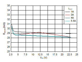 Figure 6-2 ON-Resistance vs Supply
Voltage
Figure 6-2 ON-Resistance vs Supply
VoltageFigure 6-4 IN Quiescent Current vs
Supply Voltage
Figure 6-6 IN Undervoltage Threshold
vs Temperature
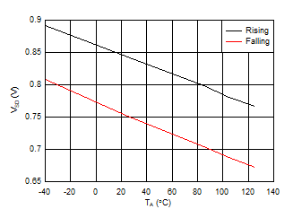 Figure 6-8 EN/UVLO Shutdown Threshold vs Temperature
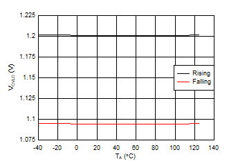 Figure 6-10 OVLO Threshold vs
Temperature
Figure 6-10 OVLO Threshold vs
TemperatureFigure 6-12 Reverse Comparator
Threshold vs Temperature
Figure 6-14 Forward Regulation Voltage
vs Supply Voltage
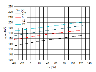 Figure 6-16 OUT Leakage Current During
ON-State Reverse Current Blocking
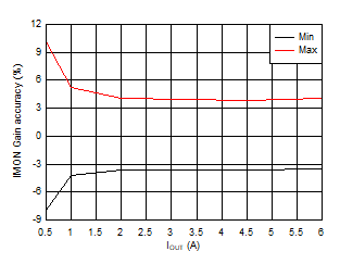 Figure 6-18 Analog
Current Monitor Gain Accuracy
 Figure 6-20 Analog Current Monitor
Gain vs Load Current
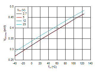 Figure 6-22 Steady State Fast-Trip
Comparator Threshold vs Temperature
Figure 6-22 Steady State Fast-Trip
Comparator Threshold vs TemperatureFigure 6-24 Time to Thermal Shut-Down
During Inrush State
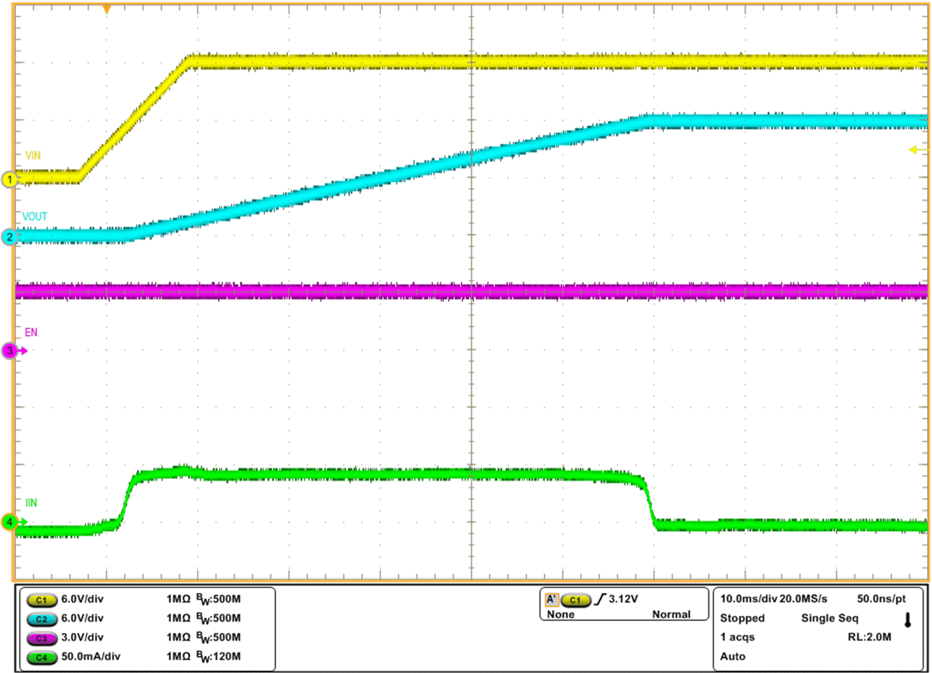
| VEN/UVLO = 3 V, COUT = 220 μF, CdVdt = 10 nF, VIN ramped up to 12 V |
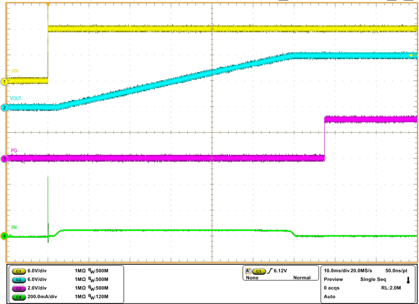
| COUT = 220 μF, CdVdt = 10 nF, EN/UVLO connected to IN through resistor ladder, 12 V hot-plugged to IN |
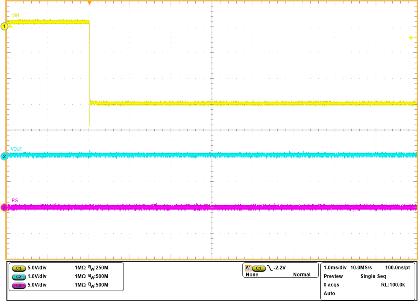
| COUT = 220 μF, PG pulled up to 3 V, -15 V hot-plugged to IN |
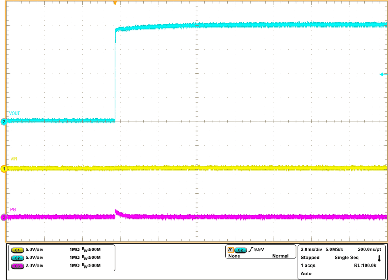
| IN= Open, COUT = 220 μF, PG pulled up to 3 V, 20 V hot-plugged to OUT |
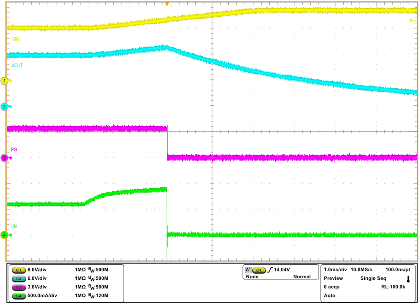
| COUT = 220 μF, ROUT = 20 Ω, OVLO threshold = 13.2 V, VIN ramped up from 12 V to 16 V |
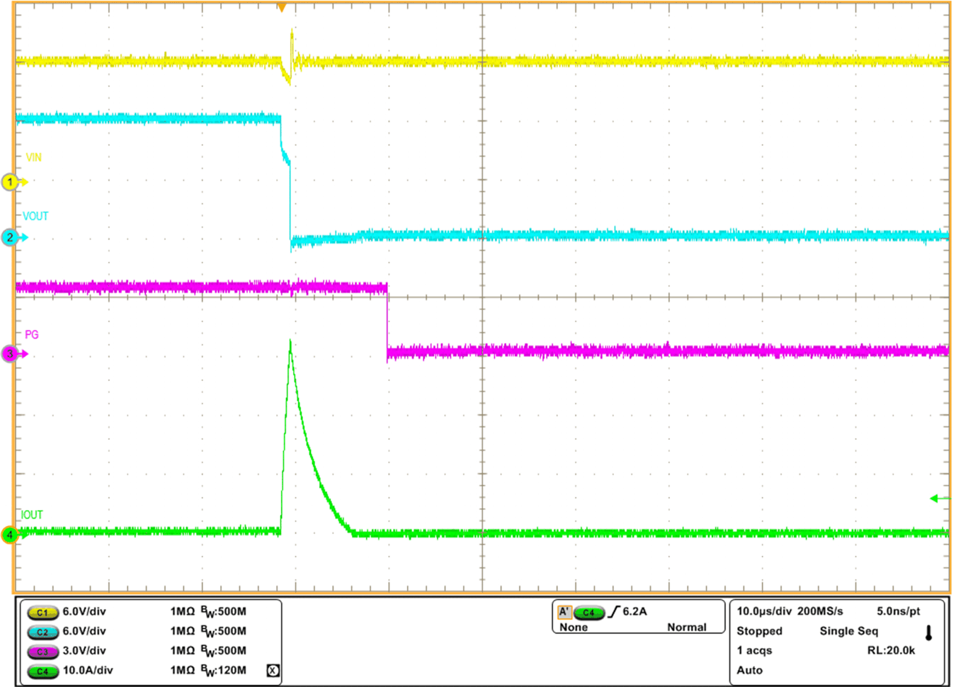
| VIN = 12 V, COUT = Open, OUT stepped from Open → Short-circuit to GND |
Figure 6-3 Forward Voltage Drop vs
Load Current
Figure 6-5 IN Quiescent Current vs
Temperature
Figure 6-7 EN/UVLO Threshold vs
Temperature
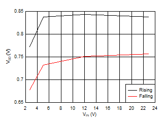 Figure 6-9 EN/UVLO Shutdown Threshold
vs Supply Voltage
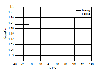 Figure 6-11 PGTH Threshold vs
Temperature
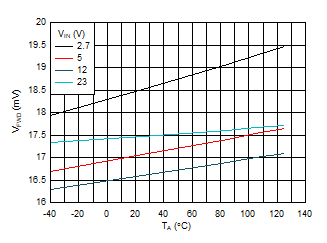 Figure 6-13 Forward Regulation Voltage
vs Temperature
Figure 6-13 Forward Regulation Voltage
vs TemperatureFigure 6-15 Forward Comparator
Threshold vs Temperature
Figure 6-17 Reverse Leakage Current During OFF-State
Figure 6-19 Analog Current Monitor
gain vs Temperature
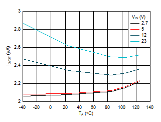 Figure 6-21 DVDT Charging Current vs
Temperature
Figure 6-21 DVDT Charging Current vs
TemperatureFigure 6-23 Steady
State Fast-Trip Current Threshold vs
Temperature
Figure 6-25 Time to thermal Shut-Down
During Steady State
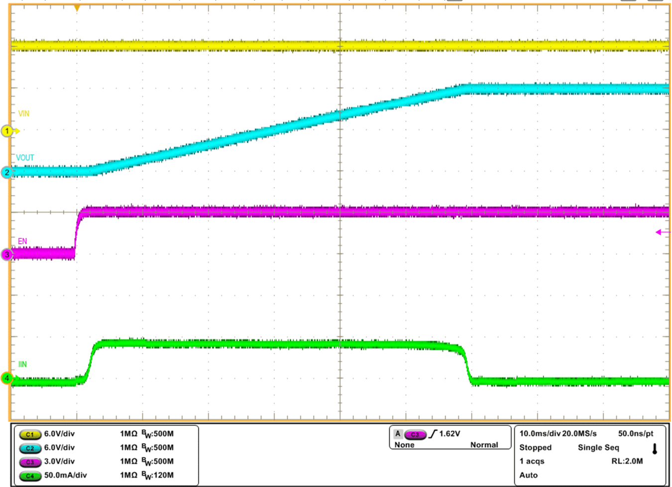
| VIN = 12 V, COUT = 220 μF, CdVdt = 10 nF, VEN/UVLO stepped up to 3 V |
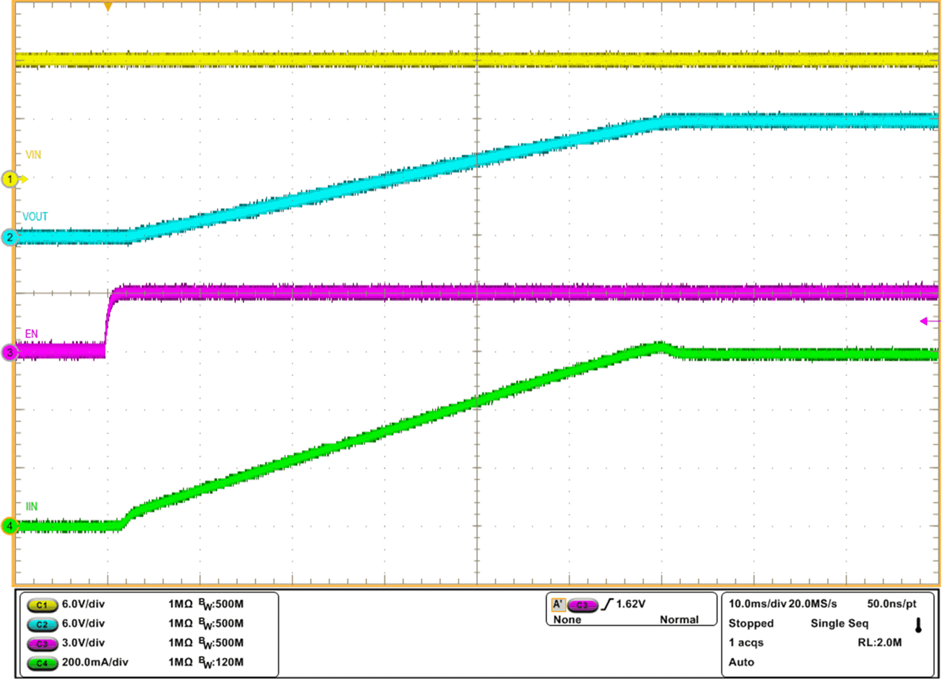
| VIN = 12 V, ROUT = 20 Ω, COUT = 220 μF, CdVdt = 10 nF, VEN/UVLO stepped up to 3 V |
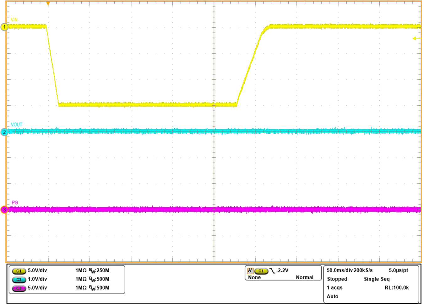
| COUT = 220 μF, PG pulled up to 3 V, VIN ramped down from 0 V to -15 V and then ramped up to 0 V |
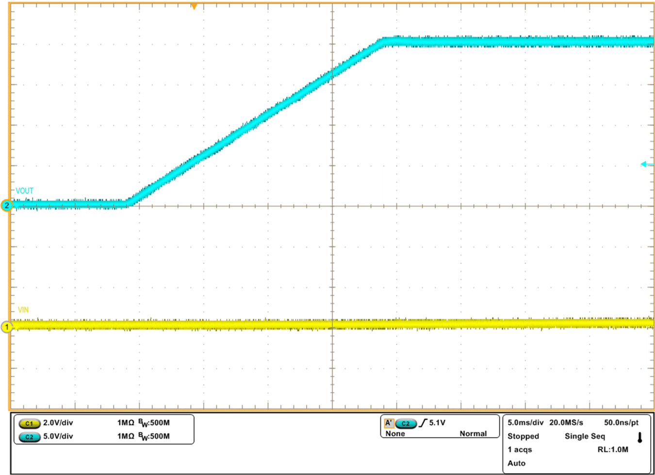
| IN= Open, COUT = 220 μF, PG pulled up to 3 V, VOUT ramped up from 0 V to 20 V |
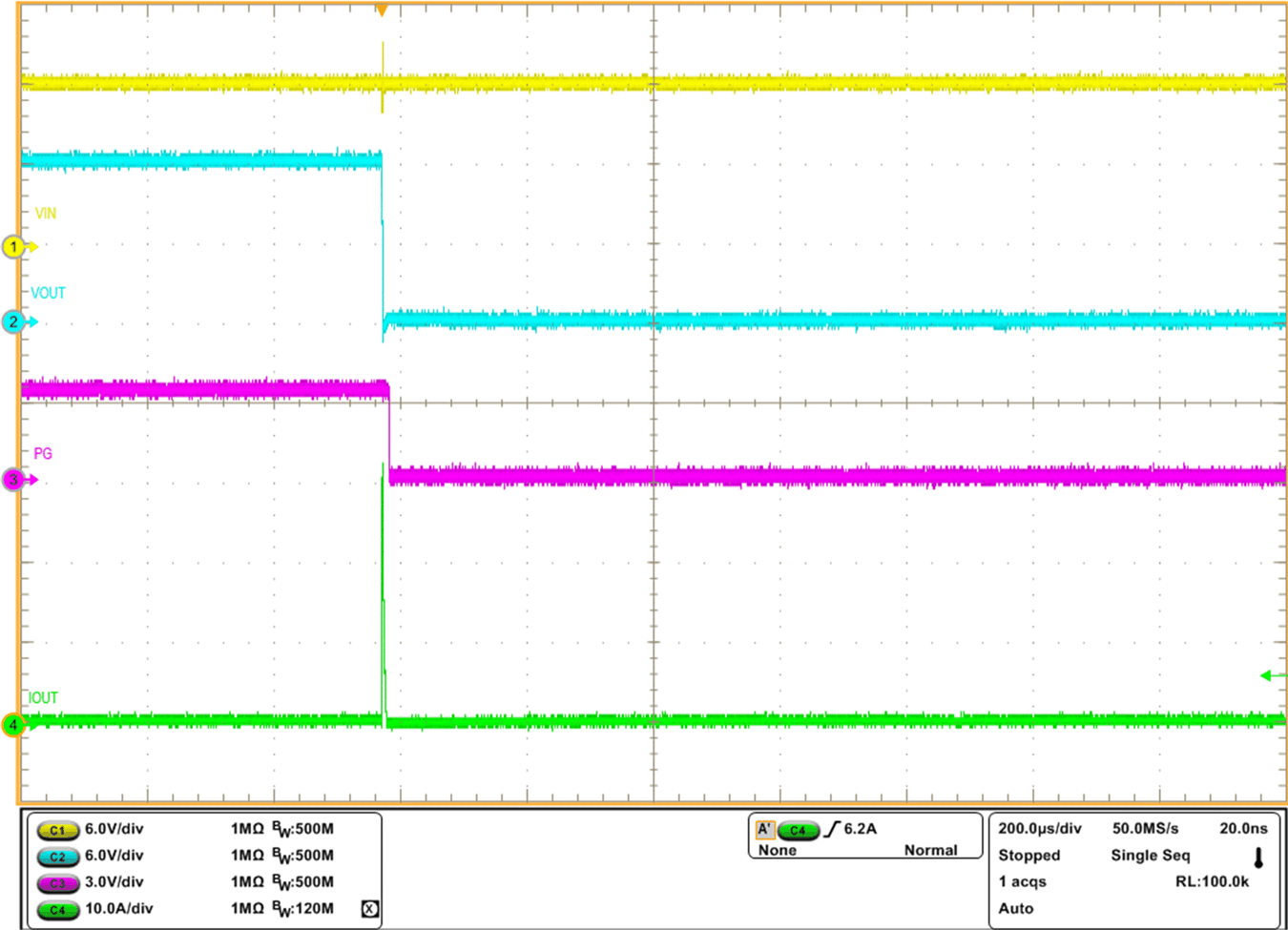
| VIN = 12 V, COUT = Open, OUT stepped from Open → Short-circuit to GND |