JAJSK72A june   2020  – october 2020 UCC23514

PRODUCTION DATA  

  1.   1
  2. 特長
  3. アプリケーション
  4. 概要
  5. Revision History
  6. Pin Configuration and Function
    1.     Pin Functions for UCC23514E
    2.     Pin Functions for UCC23514M
    3.     Pin Functions for UCC23514S
    4.     Pin Functions for UCC23514V
  7. Specifications
    1. 6.1  Absolute Maximum Ratings
    2. 6.2  ESD Ratings
    3. 6.3  Recommended Operating Conditions
    4. 6.4  Thermal Information
    5. 6.5  Power Ratings
    6. 6.6  Insulation Specifications
    7. 6.7  Safety-Related Certifications
    8. 6.8  Safety Limiting Values
    9. 6.9  Electrical Characteristics
    10. 6.10 Switching Characteristics
    11. 6.11 Insulation Characteristics
    12. 6.12 Typical Characteristics
  8. Parameter Measurement Information
    1. 7.1 Propagation Delay, rise time and fall time
    2. 7.2 IOH and IOL testing
    3. 7.3 CMTI Testing
  9. Detailed Description
    1. 8.1 Overview
    2. 8.2 Functional Block Diagram
    3. 8.3 Feature Description
      1. 8.3.1 Power Supply
      2. 8.3.2 Input Stage
      3. 8.3.3 Output Stage
      4. 8.3.4 Protection Features
        1. 8.3.4.1 Undervoltage Lockout (UVLO)
        2. 8.3.4.2 Active Pulldown
        3. 8.3.4.3 Short-Circuit Clamping
        4. 8.3.4.4 Active Miller Clamp (UCC23514M)
    4. 8.4 Device Functional Modes
      1. 8.4.1 ESD Structure
  10. Application and Implementation
    1. 9.1 Application Information
    2. 9.2 Typical Application
      1. 9.2.1 Design Requirements
      2. 9.2.2 Detailed Design Procedure
        1. 9.2.2.1 Selecting the Input Resistor
        2. 9.2.2.2 Gate-Driver Output Resistor
        3. 9.2.2.3 Estimate Gate-Driver Power Loss
        4. 9.2.2.4 Estimating Junction Temperature
        5. 9.2.2.5 Selecting VCC Capacitor
  11. 10Power Supply Recommendations
  12. 11Layout
    1. 11.1 Layout Guidelines
    2. 11.2 PCB Material
  13. 12Mechanical, Packaging, and Orderable Information

Typical Characteristics

VCC= 15 V, 1-µF capacitor from VCC to VEE, CLOAD = 1 nF for timing tests and 180nF for IOH and IOL tests, TJ = –40°C to +150°C, (unless otherwise noted)
GUID-1233B7F5-A855-48F5-B6D0-3478537E0DE4-low.gif
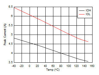
CLOAD = 180-nF
Figure 6-2 Output Drive currents versus Temperature
GUID-41BF19C3-8E0B-4DAB-87B4-C684844E4A66-low.gif
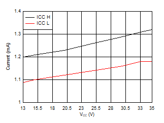
Figure 6-4 Supply current versus Supply Voltage
GUID-09382135-0AD9-460E-94C5-36B7A779B8B7-low.gif
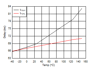
CLOAD = 1-nF
Figure 6-6 Propagation delay versus Temperature
GUID-E5764D64-F5FB-4DB1-B6A6-A9E7B0AA29A8-low.gif
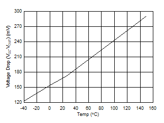
IOUT = 0mA
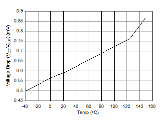
Figure 6-8 VOH (No Load) versus Temperature
GUID-AA9C16B2-324D-4D0F-AFC6-3A41CA7FD8D3-low.gif
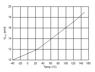
IOUT = 20mA (sinking)
Figure 6-10 VOL versus Temperature
GUID-A58E43CB-7919-41C0-A696-712F1299BDB9-low.gif
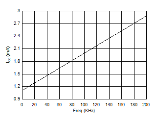
Figure 6-12 Supply current versus Frequency
GUID-D4D7D7C4-6E3B-4595-8553-AC394AD7F9DB-low.gif
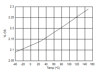
IF = 10mA
Figure 6-14 Forward voltage drop versus Temperature
GUID-F5926BF7-2DCA-4DF9-AE4D-EE3582F8C62E-low.gif
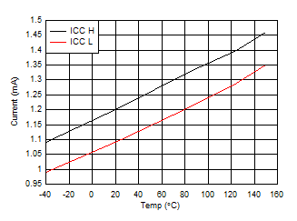
Figure 6-3 Supply currents versus Temperature
GUID-02D6B50A-16E7-4FD2-A349-F387CFE253FE-low.gif
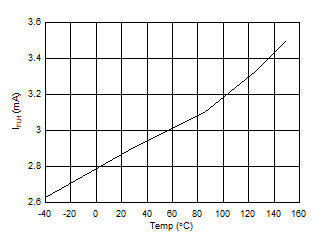
Figure 6-5 Forward threshold current versus Temperature
GUID-633F7E0F-9612-4673-B338-60E22216E176-low.gif
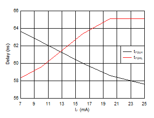
CLOAD = 1-nF
Figure 6-7 Propagation delay versus Forward current
GUID-082ABEBC-B614-4D70-9BEF-50F8B2E4B2A5-low.gif
IOUT = 20mA (sourcing)
Figure 6-9 VOH (20mA Load) versus Temperature
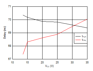
GUID-D4B9A130-5F7D-46B6-9191-52AC94BF6C98-low.gif
Figure 6-11 Propagation delay versus Supply voltage
GUID-F723E995-2D3E-4BBB-92F1-22BB66A9BDAA-low.gif
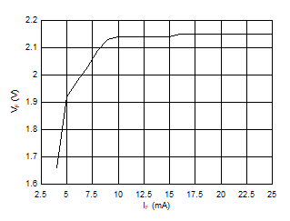
TA = 25°C
Figure 6-13 Forward current versus Forward voltage drop