JAJSKR8B October 2019 – March 2022 TCAN1144-Q1 , TCAN1145-Q1 , TCAN1146-Q1
PRODUCTION DATA
- 1 特長
- 2 アプリケーション
- 3 概要
- 4 Revision History
- 5 概要 (続き)
- 6 Device Comparison Table
- 7 Pin Configuration and Functions
- 8 Specifications
- 9 Parameter Measurement Information
-
10Detailed Description
- 10.1 Overview
- 10.2 Functional Block Diagram
- 10.3 Feature Description
- 10.4
Device Functional Modes
- 10.4.1 Normal Mode
- 10.4.2 Standby Mode
- 10.4.3 Listen Only Mode
- 10.4.4 Sleep Mode
- 10.4.5
Selective Wake-up
- 10.4.5.1 Selective Wake Mode (TCAN1145-Q1 and TCAN1146-Q1)
- 10.4.5.2 Frame Detection (TCAN1145-Q1 and TCAN1146-Q1)
- 10.4.5.3 Wake-Up Frame (WUF) Validation (TCAN1145-Q1 and TCAN1146-Q1)
- 10.4.5.4 WUF ID Validation (TCAN1145-Q1 and TCAN1146-Q1)
- 10.4.5.5 WUF DLC Validation (TCAN1145-Q1 and TCAN1146-Q1)
- 10.4.5.6 WUF Data Validation (TCAN1145-Q1 and TCAN1146-Q1)
- 10.4.5.7 Frame error counter (TCAN1145-Q1 and TCAN1146-Q1)
- 10.4.5.8 CAN FD Frame Tolerance (TCAN1145-Q1 and TCAN1146-Q1)
- 10.4.6 Fail-safe Features
- 10.4.7
Protection Features
- 10.4.7.1 Driver and Receiver Function
- 10.4.7.2 Floating Terminals
- 10.4.7.3 TXD Dominant Time Out (DTO)
- 10.4.7.4 CAN Bus Short Circuit Current Limiting
- 10.4.7.5 Thermal Shutdown
- 10.4.7.6 Under-Voltage Lockout (UVLO) and Unpowered Device
- 10.4.7.7 Watchdog (TCAN1144-Q1 and TCAN1146-Q1)
- 10.4.8 Bus Fault Detection and Communication (TCAN1144-Q1 and TCAN1146-Q1)
- 10.4.9 SPI Communication
- 10.5 Programming
- 10.6
Register Maps
- 10.6.1 DEVICE_ID_y Register (Address = 0h + formula) [reset = value]
- 10.6.2 REV_ID_MAJOR Register (Address = 8h) [reset = 01h]
- 10.6.3 REV_ID_MINOR Register (Address = 9h) [reset = 00h]
- 10.6.4 SPI_RSVD_x Register (Address = Ah + formula) [reset = 00h]
- 10.6.5 Scratch_Pad_SPI Register (Address = Fh) [reset = 00h]
- 10.6.6 MODE_CNTRL Register (Address = 10h) [reset = 04h]
- 10.6.7 WAKE_PIN_CONFIG Register (Address = 11h) [reset = 4h]
- 10.6.8 PIN_CONFIG Register (Address = 12h) [reset = 00h]
- 10.6.9 WD_CONFIG_1 Register (Address = 13h) [reset = 15h]
- 10.6.10 WD_CONFIG_2 Register (Address = 14h) [reset = 02h]
- 10.6.11 WD_INPUT_TRIG Register (Address = 15h) [reset = 00h]
- 10.6.12 WD_RST_PULSE Register (Address = 16h) [reset = 07h]
- 10.6.13 FSM_CONFIG Register (Address = 17h) [reset = 00h]
- 10.6.14 FSM_CNTR Register (Address = 18h) [reset = 00h]
- 10.6.15 DEVICE_RST Register (Address = 19h) [reset = 00h]
- 10.6.16 DEVICE_CONFIG1 Register (Address = 1Ah) [reset = 00h]
- 10.6.17 DEVICE_CONFIG2 Register (Address = 1Bh) [reset = 0h]
- 10.6.18 SWE_DIS Register (Address 1Ch) [reset = 04h]
- 10.6.19 SDO_CONFIG Register (Address = 29h) [reset = 00h]
- 10.6.20 WD_QA_CONFIG Register (Address = 2Dh) [reset = 00h]
- 10.6.21 WD_QA_ANSWER Register (Address = 2Eh) [reset = 00h]
- 10.6.22 WD_QA_QUESTION Register (Address = 2Fh) [reset = 00h]
- 10.6.23 SW_ID1 Register (Address = 30h) [reset = 00h]
- 10.6.24 SW_ID2 Register (Address = 31h) [reset = 00h]
- 10.6.25 SW_ID3 Register (Address = 32h) [reset = 00h]
- 10.6.26 SW_ID4 Register (Address = 33h) [reset = 00h]
- 10.6.27 SW_ID_MASK1 Register (Address = 34h) [reset = 00h]
- 10.6.28 SW_ID_MASK2 Register (Address = 35h) [reset = 00h]
- 10.6.29 SW_ID_MASK3 Register (Address = 36h) [reset = 00h]
- 10.6.30 SW_ID_MASK4 Register (Address = 37h) [reset = 00h]
- 10.6.31 SW_ID_MASK_DLC Register (Address = 38h) [reset = 00h]
- 10.6.32 DATA_y Register (Address = 39h + formula) [reset = 00h]
- 10.6.33 SW_RSVD_y Register (Address = 41h + formula) [reset = 00h]
- 10.6.34 SW_CONFIG_1 Register (Address = 44h) [reset = 50h]
- 10.6.35 SW_CONFIG_2 Register (Address = 45h) [reset = 00h]
- 10.6.36 SW_CONFIG_3 Register (Address = 46h) [reset = 1Fh]
- 10.6.37 SW_CONFIG_4 Register (Address = 47h) [reset = 00h]
- 10.6.38 SW_CONFIG_RSVD_y Register (Address = 48h + formula) [reset = 00h]
- 10.6.39 INT_GLOBAL Register (Address = 50h) [reset = 00h]
- 10.6.40 INT_1 Register (Address = 51h) [reset = 00h]
- 10.6.41 INT_2 Register (Address = 52h) [reset = 40h]
- 10.6.42 INT_3 Register (Address 53h) [reset = 00h]
- 10.6.43 INT_CANBUS Register (Address = 54h) [reset = 00h]
- 10.6.44 INT_GLOBAL_ENABLE (Address = 55h) [reset = 00h]
- 10.6.45 INT_ENABLE_1 Register (Address = 56h) [reset = FFh]
- 10.6.46 INT_ENABLE_2 Register (Address = 57h) [reset = 1Fh]
- 10.6.47 INT_ENABLE_3 Register (Address = 58h) [reset = 0h]
- 10.6.48 INT_ENABLE_CANBUS Register (Address = 59h) [reset = 7Fh]
- 10.6.49 INT_RSVD_y Register (Address = 5Ah + formula) [reset = 00h]
- 11Application Information Disclaimer
- 12Power Supply Recommendations
- 13Layout
- 14Device and Documentation Support
- 15Mechanical, Packaging, and Orderable Information
10.4.8 Bus Fault Detection and Communication (TCAN1144-Q1 and TCAN1146-Q1)
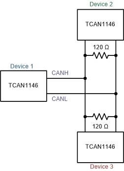
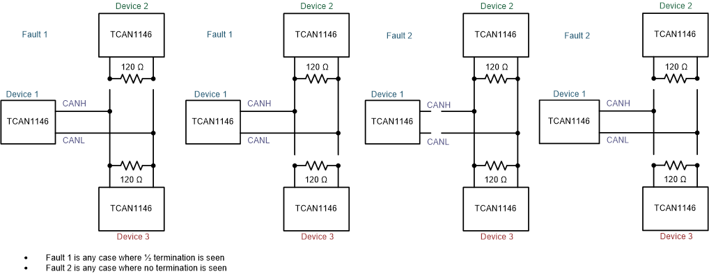
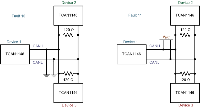
The TCAN1144-Q1 and TCAN1146-Q1 provide advanced bus fault detection. TCAN1146-Q1 is used for illustration purposes. The device can determine certain fault conditions and set a status/interrupt flag so that the MCU can understand what the fault is. Detection takes place and is recorded if the fault is present during four dominant to recessive transitions with each dominant bit being ≥ 2 µs. As with any bus architecture where termination resistors are at each end not every fault can be specified to the lowest level, meaning exact location. The fault detection circuitry is monitoring the CANH and CANL pins (currents) to determine if there is a short to battery, short to ground, short to each other or opens. From a system perspective, the location of the device can impact what fault can be detected. See Figure 10-29 as an example of node locations and how they can impact the ability to determine the actual fault location. Figure 10-30 through Figure 10-34 show the various bus faults based upon the three-node configuration. Table 10-17 shows what can be detected and by which device. Fault 1 is detected as ½ termination and Fault 2 is detected as no termination.
Bus fault detection is a system-level situation. If the fault is occurring at the ECU then the general communication of the bus is compromised. For complete coverage of a node a system level diagnostic step for each node and the ability to communicate this back to a central point is needed.
 Figure 10-29 Three-Node Example
 Figure 10-30 Open Fault 1 and 2 Examples
 Figure 10-31 Open Fault 3 and 4 Examples
 Figure 10-32 Fault 5 and 6 Examples
 Figure 10-33 Fault 7, 8 and 9 Examples
 Figure 10-34 Fault 10 and 11 Examples
| Fault # | CANH | CANL | Fault Detected |
|---|---|---|---|
| 1 | Open | Open | All positions see this fault as half termination and detect them |
| 2 | Open | Open | Depending upon open location the device detects this as no termination. |
| 3 | Open | Normal | Yes, but cannot tell the difference between it and Fault 2 and 4; Device 2 and Device 3 does not see this fault |
| 4 | Normal | Open | Yes, but cannot tell the difference between it and Fault 2 and 3; Device 2 and Device 3 does not see this fault |
| 5 | Shorted to CANL | Shorted to CANH | Yes, but not location |
| 6 | Shorted to Vbat | Normal | Yes, but not location |
| 7 | Shorted to GND | Normal | Yes, but cannot tell the difference between this and Fault 10 |
| 8 | Normal | Shorted to VBAT | Yes, but cannot tell the difference between this and Fault 11 |
| 9 | Normal | Shorted to GND | Yes, but not location |
| 10 | Shorted to GND | Shorted to GND | Yes, but cannot tell the difference between this and Fault 7 |
| 11 | Shorted to Vbat | Shorted to VBAT | Yes, but cannot tell the difference between this and Fault 8 |
| Address | BIT(S) | DEFAULT | FLAG | DESCRIPTION | FAULT DETECTED | ACCESS |
|---|---|---|---|---|---|---|
| 8'h54 | 7 | 1'b0 | RSVD | Reserved | ||
| 6 | 1'b0 | CANBUSTERMOPEN | CAN Bus has one termination point open | Fault 1 | R/WC | |
| 5 | 1'b0 | CANHCANL | CANH and CANL Shorted Together | Fault 5 | R/WC | |
| 4 | 1'b0 | CANHBAT | CANH Shorted to VBAT | Fault 6 | R/WC | |
| 3 | 1'b0 | CANLGND | CANL Shorted to GND | Fault 9 | R/WC | |
| 2 | 1'b0 | CANBUSOPEN | CAN Bus Open (One of three possible places) | Faults 2, 3 and 4 | R/WC | |
| 1 | 1'b0 | CANBUSGND | CANH Shorted to GND or Both CANH & CANL Shorted to GND | Faults 7 and 10 | R/WC | |
| 0 | 1'b0 | CANBUSBAT | CANL Shorted to VBAT or Both CANH & CANL Shorted to VBAT | Faults 8 and 11 | R/WC |