JAJSKR8B October 2019 – March 2022 TCAN1144-Q1 , TCAN1145-Q1 , TCAN1146-Q1
PRODUCTION DATA
- 1 特長
- 2 アプリケーション
- 3 概要
- 4 Revision History
- 5 概要 (続き)
- 6 Device Comparison Table
- 7 Pin Configuration and Functions
- 8 Specifications
- 9 Parameter Measurement Information
-
10Detailed Description
- 10.1 Overview
- 10.2 Functional Block Diagram
- 10.3 Feature Description
- 10.4
Device Functional Modes
- 10.4.1 Normal Mode
- 10.4.2 Standby Mode
- 10.4.3 Listen Only Mode
- 10.4.4 Sleep Mode
- 10.4.5
Selective Wake-up
- 10.4.5.1 Selective Wake Mode (TCAN1145-Q1 and TCAN1146-Q1)
- 10.4.5.2 Frame Detection (TCAN1145-Q1 and TCAN1146-Q1)
- 10.4.5.3 Wake-Up Frame (WUF) Validation (TCAN1145-Q1 and TCAN1146-Q1)
- 10.4.5.4 WUF ID Validation (TCAN1145-Q1 and TCAN1146-Q1)
- 10.4.5.5 WUF DLC Validation (TCAN1145-Q1 and TCAN1146-Q1)
- 10.4.5.6 WUF Data Validation (TCAN1145-Q1 and TCAN1146-Q1)
- 10.4.5.7 Frame error counter (TCAN1145-Q1 and TCAN1146-Q1)
- 10.4.5.8 CAN FD Frame Tolerance (TCAN1145-Q1 and TCAN1146-Q1)
- 10.4.6 Fail-safe Features
- 10.4.7
Protection Features
- 10.4.7.1 Driver and Receiver Function
- 10.4.7.2 Floating Terminals
- 10.4.7.3 TXD Dominant Time Out (DTO)
- 10.4.7.4 CAN Bus Short Circuit Current Limiting
- 10.4.7.5 Thermal Shutdown
- 10.4.7.6 Under-Voltage Lockout (UVLO) and Unpowered Device
- 10.4.7.7 Watchdog (TCAN1144-Q1 and TCAN1146-Q1)
- 10.4.8 Bus Fault Detection and Communication (TCAN1144-Q1 and TCAN1146-Q1)
- 10.4.9 SPI Communication
- 10.5 Programming
- 10.6
Register Maps
- 10.6.1 DEVICE_ID_y Register (Address = 0h + formula) [reset = value]
- 10.6.2 REV_ID_MAJOR Register (Address = 8h) [reset = 01h]
- 10.6.3 REV_ID_MINOR Register (Address = 9h) [reset = 00h]
- 10.6.4 SPI_RSVD_x Register (Address = Ah + formula) [reset = 00h]
- 10.6.5 Scratch_Pad_SPI Register (Address = Fh) [reset = 00h]
- 10.6.6 MODE_CNTRL Register (Address = 10h) [reset = 04h]
- 10.6.7 WAKE_PIN_CONFIG Register (Address = 11h) [reset = 4h]
- 10.6.8 PIN_CONFIG Register (Address = 12h) [reset = 00h]
- 10.6.9 WD_CONFIG_1 Register (Address = 13h) [reset = 15h]
- 10.6.10 WD_CONFIG_2 Register (Address = 14h) [reset = 02h]
- 10.6.11 WD_INPUT_TRIG Register (Address = 15h) [reset = 00h]
- 10.6.12 WD_RST_PULSE Register (Address = 16h) [reset = 07h]
- 10.6.13 FSM_CONFIG Register (Address = 17h) [reset = 00h]
- 10.6.14 FSM_CNTR Register (Address = 18h) [reset = 00h]
- 10.6.15 DEVICE_RST Register (Address = 19h) [reset = 00h]
- 10.6.16 DEVICE_CONFIG1 Register (Address = 1Ah) [reset = 00h]
- 10.6.17 DEVICE_CONFIG2 Register (Address = 1Bh) [reset = 0h]
- 10.6.18 SWE_DIS Register (Address 1Ch) [reset = 04h]
- 10.6.19 SDO_CONFIG Register (Address = 29h) [reset = 00h]
- 10.6.20 WD_QA_CONFIG Register (Address = 2Dh) [reset = 00h]
- 10.6.21 WD_QA_ANSWER Register (Address = 2Eh) [reset = 00h]
- 10.6.22 WD_QA_QUESTION Register (Address = 2Fh) [reset = 00h]
- 10.6.23 SW_ID1 Register (Address = 30h) [reset = 00h]
- 10.6.24 SW_ID2 Register (Address = 31h) [reset = 00h]
- 10.6.25 SW_ID3 Register (Address = 32h) [reset = 00h]
- 10.6.26 SW_ID4 Register (Address = 33h) [reset = 00h]
- 10.6.27 SW_ID_MASK1 Register (Address = 34h) [reset = 00h]
- 10.6.28 SW_ID_MASK2 Register (Address = 35h) [reset = 00h]
- 10.6.29 SW_ID_MASK3 Register (Address = 36h) [reset = 00h]
- 10.6.30 SW_ID_MASK4 Register (Address = 37h) [reset = 00h]
- 10.6.31 SW_ID_MASK_DLC Register (Address = 38h) [reset = 00h]
- 10.6.32 DATA_y Register (Address = 39h + formula) [reset = 00h]
- 10.6.33 SW_RSVD_y Register (Address = 41h + formula) [reset = 00h]
- 10.6.34 SW_CONFIG_1 Register (Address = 44h) [reset = 50h]
- 10.6.35 SW_CONFIG_2 Register (Address = 45h) [reset = 00h]
- 10.6.36 SW_CONFIG_3 Register (Address = 46h) [reset = 1Fh]
- 10.6.37 SW_CONFIG_4 Register (Address = 47h) [reset = 00h]
- 10.6.38 SW_CONFIG_RSVD_y Register (Address = 48h + formula) [reset = 00h]
- 10.6.39 INT_GLOBAL Register (Address = 50h) [reset = 00h]
- 10.6.40 INT_1 Register (Address = 51h) [reset = 00h]
- 10.6.41 INT_2 Register (Address = 52h) [reset = 40h]
- 10.6.42 INT_3 Register (Address 53h) [reset = 00h]
- 10.6.43 INT_CANBUS Register (Address = 54h) [reset = 00h]
- 10.6.44 INT_GLOBAL_ENABLE (Address = 55h) [reset = 00h]
- 10.6.45 INT_ENABLE_1 Register (Address = 56h) [reset = FFh]
- 10.6.46 INT_ENABLE_2 Register (Address = 57h) [reset = 1Fh]
- 10.6.47 INT_ENABLE_3 Register (Address = 58h) [reset = 0h]
- 10.6.48 INT_ENABLE_CANBUS Register (Address = 59h) [reset = 7Fh]
- 10.6.49 INT_RSVD_y Register (Address = 5Ah + formula) [reset = 00h]
- 11Application Information Disclaimer
- 12Power Supply Recommendations
- 13Layout
- 14Device and Documentation Support
- 15Mechanical, Packaging, and Orderable Information
10.4.9.4 SPI Serial Data Output (SDO):
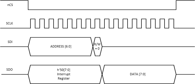
This pin is high impedance until the SPI output is enabled via nCS. Once the SPI is enabled by a low on nCS, the SDO is immediately driven high or low showing the global interrupt register 8'h50, bit 7. The Global Interrupt register, INT_GLOBAL, is the first byte to be shifted out. The SDO pin provides data out from the device to the processor. For a write command this is the only data that will be provided on the SDO pin. For a read command the one to three bytes of data from successive address will be provided on the SDO line. Figure 10-38 and Figure 10-39 shows examples of a single address read and of a three sequential address read utilizing the 32-bit burst read. The 32-bit burst read shows the global interrupt register followed by the three requested data bytes.
 Figure 10-38 SPI Read
 Figure 10-39 32-bit SPI Burst
Read.
Example on how to read three bytes of data from one SPI read command.
If a read happens faster than 2 µs after a write the global fault flag status may not reflect any status change that the write may have initiated.