JAJSKR8B October 2019 – March 2022 TCAN1144-Q1 , TCAN1145-Q1 , TCAN1146-Q1
PRODUCTION DATA
- 1 特長
- 2 アプリケーション
- 3 概要
- 4 Revision History
- 5 概要 (続き)
- 6 Device Comparison Table
- 7 Pin Configuration and Functions
- 8 Specifications
- 9 Parameter Measurement Information
-
10Detailed Description
- 10.1 Overview
- 10.2 Functional Block Diagram
- 10.3 Feature Description
- 10.4
Device Functional Modes
- 10.4.1 Normal Mode
- 10.4.2 Standby Mode
- 10.4.3 Listen Only Mode
- 10.4.4 Sleep Mode
- 10.4.5
Selective Wake-up
- 10.4.5.1 Selective Wake Mode (TCAN1145-Q1 and TCAN1146-Q1)
- 10.4.5.2 Frame Detection (TCAN1145-Q1 and TCAN1146-Q1)
- 10.4.5.3 Wake-Up Frame (WUF) Validation (TCAN1145-Q1 and TCAN1146-Q1)
- 10.4.5.4 WUF ID Validation (TCAN1145-Q1 and TCAN1146-Q1)
- 10.4.5.5 WUF DLC Validation (TCAN1145-Q1 and TCAN1146-Q1)
- 10.4.5.6 WUF Data Validation (TCAN1145-Q1 and TCAN1146-Q1)
- 10.4.5.7 Frame error counter (TCAN1145-Q1 and TCAN1146-Q1)
- 10.4.5.8 CAN FD Frame Tolerance (TCAN1145-Q1 and TCAN1146-Q1)
- 10.4.6 Fail-safe Features
- 10.4.7
Protection Features
- 10.4.7.1 Driver and Receiver Function
- 10.4.7.2 Floating Terminals
- 10.4.7.3 TXD Dominant Time Out (DTO)
- 10.4.7.4 CAN Bus Short Circuit Current Limiting
- 10.4.7.5 Thermal Shutdown
- 10.4.7.6 Under-Voltage Lockout (UVLO) and Unpowered Device
- 10.4.7.7 Watchdog (TCAN1144-Q1 and TCAN1146-Q1)
- 10.4.8 Bus Fault Detection and Communication (TCAN1144-Q1 and TCAN1146-Q1)
- 10.4.9 SPI Communication
- 10.5 Programming
- 10.6
Register Maps
- 10.6.1 DEVICE_ID_y Register (Address = 0h + formula) [reset = value]
- 10.6.2 REV_ID_MAJOR Register (Address = 8h) [reset = 01h]
- 10.6.3 REV_ID_MINOR Register (Address = 9h) [reset = 00h]
- 10.6.4 SPI_RSVD_x Register (Address = Ah + formula) [reset = 00h]
- 10.6.5 Scratch_Pad_SPI Register (Address = Fh) [reset = 00h]
- 10.6.6 MODE_CNTRL Register (Address = 10h) [reset = 04h]
- 10.6.7 WAKE_PIN_CONFIG Register (Address = 11h) [reset = 4h]
- 10.6.8 PIN_CONFIG Register (Address = 12h) [reset = 00h]
- 10.6.9 WD_CONFIG_1 Register (Address = 13h) [reset = 15h]
- 10.6.10 WD_CONFIG_2 Register (Address = 14h) [reset = 02h]
- 10.6.11 WD_INPUT_TRIG Register (Address = 15h) [reset = 00h]
- 10.6.12 WD_RST_PULSE Register (Address = 16h) [reset = 07h]
- 10.6.13 FSM_CONFIG Register (Address = 17h) [reset = 00h]
- 10.6.14 FSM_CNTR Register (Address = 18h) [reset = 00h]
- 10.6.15 DEVICE_RST Register (Address = 19h) [reset = 00h]
- 10.6.16 DEVICE_CONFIG1 Register (Address = 1Ah) [reset = 00h]
- 10.6.17 DEVICE_CONFIG2 Register (Address = 1Bh) [reset = 0h]
- 10.6.18 SWE_DIS Register (Address 1Ch) [reset = 04h]
- 10.6.19 SDO_CONFIG Register (Address = 29h) [reset = 00h]
- 10.6.20 WD_QA_CONFIG Register (Address = 2Dh) [reset = 00h]
- 10.6.21 WD_QA_ANSWER Register (Address = 2Eh) [reset = 00h]
- 10.6.22 WD_QA_QUESTION Register (Address = 2Fh) [reset = 00h]
- 10.6.23 SW_ID1 Register (Address = 30h) [reset = 00h]
- 10.6.24 SW_ID2 Register (Address = 31h) [reset = 00h]
- 10.6.25 SW_ID3 Register (Address = 32h) [reset = 00h]
- 10.6.26 SW_ID4 Register (Address = 33h) [reset = 00h]
- 10.6.27 SW_ID_MASK1 Register (Address = 34h) [reset = 00h]
- 10.6.28 SW_ID_MASK2 Register (Address = 35h) [reset = 00h]
- 10.6.29 SW_ID_MASK3 Register (Address = 36h) [reset = 00h]
- 10.6.30 SW_ID_MASK4 Register (Address = 37h) [reset = 00h]
- 10.6.31 SW_ID_MASK_DLC Register (Address = 38h) [reset = 00h]
- 10.6.32 DATA_y Register (Address = 39h + formula) [reset = 00h]
- 10.6.33 SW_RSVD_y Register (Address = 41h + formula) [reset = 00h]
- 10.6.34 SW_CONFIG_1 Register (Address = 44h) [reset = 50h]
- 10.6.35 SW_CONFIG_2 Register (Address = 45h) [reset = 00h]
- 10.6.36 SW_CONFIG_3 Register (Address = 46h) [reset = 1Fh]
- 10.6.37 SW_CONFIG_4 Register (Address = 47h) [reset = 00h]
- 10.6.38 SW_CONFIG_RSVD_y Register (Address = 48h + formula) [reset = 00h]
- 10.6.39 INT_GLOBAL Register (Address = 50h) [reset = 00h]
- 10.6.40 INT_1 Register (Address = 51h) [reset = 00h]
- 10.6.41 INT_2 Register (Address = 52h) [reset = 40h]
- 10.6.42 INT_3 Register (Address 53h) [reset = 00h]
- 10.6.43 INT_CANBUS Register (Address = 54h) [reset = 00h]
- 10.6.44 INT_GLOBAL_ENABLE (Address = 55h) [reset = 00h]
- 10.6.45 INT_ENABLE_1 Register (Address = 56h) [reset = FFh]
- 10.6.46 INT_ENABLE_2 Register (Address = 57h) [reset = 1Fh]
- 10.6.47 INT_ENABLE_3 Register (Address = 58h) [reset = 0h]
- 10.6.48 INT_ENABLE_CANBUS Register (Address = 59h) [reset = 7Fh]
- 10.6.49 INT_RSVD_y Register (Address = 5Ah + formula) [reset = 00h]
- 11Application Information Disclaimer
- 12Power Supply Recommendations
- 13Layout
- 14Device and Documentation Support
- 15Mechanical, Packaging, and Orderable Information
10.4.4.1 Bus Wake via RXD Request (BWRR) in Sleep Mode
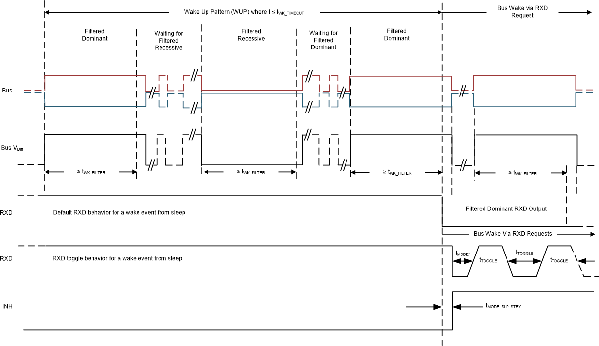
The TCAN114x-Q1 supports low power sleep and standby modes and uses a wake up from the CAN bus mechanism called bus wake via RXD Request (BWRR). Once this pattern is received, the TCAN114x-Q1 automatically switches to standby mode from sleep mode and inserts an interrupt onto the nINT pin, if enabled, to indicate to a host microprocessor that the bus is active, and the processor should wake up and service the TCAN114x-Q1. The low power receiver and bus monitor are enabled in sleep mode to allow for RXD Wake Requests via the CAN bus. A wake-up request is output to the RXD (driven low) as shown in Figure 10-12. The external CAN FD controller monitors RXD for transitions (high to low) and reactivates the device to normal mode based on the RXD Wake Request. The CAN bus terminals are weakly pulled to GND during this mode, prior to BWRR if tSILENCE is expired, see Figure 9-2.
This device uses the wake-up pattern (WUP) from ISO 11898-2: 2016 to qualify bus traffic into a request to wake the host microprocessor. The bus wake request is signaled to the integrated CAN FD controller by a falling edge and low corresponding to a “filtered” bus dominant on the RXD terminal (BWRR).
The wake-up pattern (WUP) consists of
- A filtered dominant bus of at least tWK_FILTER followed by
- A filtered recessive bus time of at least tWK_FILTER followed by
- A second filtered dominant bus time of at least tWK_FILTER
Once the WUP is detected, the device starts issuing wake up requests (BWRR) on the RXD pin. The behavior of this pin is determined by register h'12[2]. If h'12[2] = 0 the RXD pin is pulled low once the WUP pattern has been received that meets the dominant, recessive, dominant filtered times. The first filtered dominant initiates the WUP and the bus monitor is now waiting on a filtered recessive; other bus traffic does not reset the bus monitor. Once a filtered recessive is received, the bus monitor is now waiting on a filtered dominant and again, other bus traffic does not reset the bus monitor. Immediately upon receiving of the second filtered dominant, the bus monitor recognizes the WUP and transition to BWRR output.
For a dominant or recessive to be considered “filtered”, the bus must be in that state for more than tWK_FILTER time. Due to variability in the tWK_FILTER the following scenarios are applicable.
- Bus state times less than tWK_FILTER(MIN) are never detected as part of a WUP, and thus no BWRR is generated.
- Bus state times between tWK_FILTER(MIN) and tWK_FILTER(MAX) may be detected as part of a WUP and a BWRR may be generated.
- Bus state times more than tWK_FILTER(MAX) is always detected as part of a WUP; thus, a BWRR is always generated.
See Figure 10-12 for the timing diagram of the WUP.
The pattern and tWK_FILTER time used for the WUP and BWRR prevents noise and a bus stuck dominant fault from causing false wake requests while allowing any CAN or CAN FD message to initiate a BWRR. If the device is switched to normal mode or an under voltage event occurs on VCC the BWRR is lost. The WUP pattern must take place within the tWK_TIMEOUT time; otherwise, the device is in a state waiting for the next recessive and then a valid WUP pattern.
If h'12[2] = 1 the RXD pin toggles low to high to low for tTOGGLE = 10 µs until the device is put into normal or listen mode. BWRR is active in standby mode upon power up and once coming out of sleep mode or certain fail-safe mode conditions. If a SPI write puts the device into standby mode, the RXD pin is high until a wake event takes place. The RXD pin then behaves like it would when waking up from sleep mode.
 Figure 10-12 Wake Up Pattern (WUP) and Bus Wake via RXD Request (BWRR)
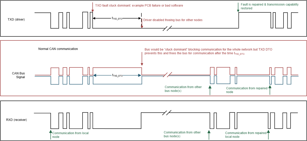
 Figure 10-13 Example timing diagram with TXD DTO