JAJSKR8B October 2019 – March 2022 TCAN1144-Q1 , TCAN1145-Q1 , TCAN1146-Q1
PRODUCTION DATA
- 1 特長
- 2 アプリケーション
- 3 概要
- 4 Revision History
- 5 概要 (続き)
- 6 Device Comparison Table
- 7 Pin Configuration and Functions
- 8 Specifications
- 9 Parameter Measurement Information
-
10Detailed Description
- 10.1 Overview
- 10.2 Functional Block Diagram
- 10.3 Feature Description
- 10.4
Device Functional Modes
- 10.4.1 Normal Mode
- 10.4.2 Standby Mode
- 10.4.3 Listen Only Mode
- 10.4.4 Sleep Mode
- 10.4.5
Selective Wake-up
- 10.4.5.1 Selective Wake Mode (TCAN1145-Q1 and TCAN1146-Q1)
- 10.4.5.2 Frame Detection (TCAN1145-Q1 and TCAN1146-Q1)
- 10.4.5.3 Wake-Up Frame (WUF) Validation (TCAN1145-Q1 and TCAN1146-Q1)
- 10.4.5.4 WUF ID Validation (TCAN1145-Q1 and TCAN1146-Q1)
- 10.4.5.5 WUF DLC Validation (TCAN1145-Q1 and TCAN1146-Q1)
- 10.4.5.6 WUF Data Validation (TCAN1145-Q1 and TCAN1146-Q1)
- 10.4.5.7 Frame error counter (TCAN1145-Q1 and TCAN1146-Q1)
- 10.4.5.8 CAN FD Frame Tolerance (TCAN1145-Q1 and TCAN1146-Q1)
- 10.4.6 Fail-safe Features
- 10.4.7
Protection Features
- 10.4.7.1 Driver and Receiver Function
- 10.4.7.2 Floating Terminals
- 10.4.7.3 TXD Dominant Time Out (DTO)
- 10.4.7.4 CAN Bus Short Circuit Current Limiting
- 10.4.7.5 Thermal Shutdown
- 10.4.7.6 Under-Voltage Lockout (UVLO) and Unpowered Device
- 10.4.7.7 Watchdog (TCAN1144-Q1 and TCAN1146-Q1)
- 10.4.8 Bus Fault Detection and Communication (TCAN1144-Q1 and TCAN1146-Q1)
- 10.4.9 SPI Communication
- 10.5 Programming
- 10.6
Register Maps
- 10.6.1 DEVICE_ID_y Register (Address = 0h + formula) [reset = value]
- 10.6.2 REV_ID_MAJOR Register (Address = 8h) [reset = 01h]
- 10.6.3 REV_ID_MINOR Register (Address = 9h) [reset = 00h]
- 10.6.4 SPI_RSVD_x Register (Address = Ah + formula) [reset = 00h]
- 10.6.5 Scratch_Pad_SPI Register (Address = Fh) [reset = 00h]
- 10.6.6 MODE_CNTRL Register (Address = 10h) [reset = 04h]
- 10.6.7 WAKE_PIN_CONFIG Register (Address = 11h) [reset = 4h]
- 10.6.8 PIN_CONFIG Register (Address = 12h) [reset = 00h]
- 10.6.9 WD_CONFIG_1 Register (Address = 13h) [reset = 15h]
- 10.6.10 WD_CONFIG_2 Register (Address = 14h) [reset = 02h]
- 10.6.11 WD_INPUT_TRIG Register (Address = 15h) [reset = 00h]
- 10.6.12 WD_RST_PULSE Register (Address = 16h) [reset = 07h]
- 10.6.13 FSM_CONFIG Register (Address = 17h) [reset = 00h]
- 10.6.14 FSM_CNTR Register (Address = 18h) [reset = 00h]
- 10.6.15 DEVICE_RST Register (Address = 19h) [reset = 00h]
- 10.6.16 DEVICE_CONFIG1 Register (Address = 1Ah) [reset = 00h]
- 10.6.17 DEVICE_CONFIG2 Register (Address = 1Bh) [reset = 0h]
- 10.6.18 SWE_DIS Register (Address 1Ch) [reset = 04h]
- 10.6.19 SDO_CONFIG Register (Address = 29h) [reset = 00h]
- 10.6.20 WD_QA_CONFIG Register (Address = 2Dh) [reset = 00h]
- 10.6.21 WD_QA_ANSWER Register (Address = 2Eh) [reset = 00h]
- 10.6.22 WD_QA_QUESTION Register (Address = 2Fh) [reset = 00h]
- 10.6.23 SW_ID1 Register (Address = 30h) [reset = 00h]
- 10.6.24 SW_ID2 Register (Address = 31h) [reset = 00h]
- 10.6.25 SW_ID3 Register (Address = 32h) [reset = 00h]
- 10.6.26 SW_ID4 Register (Address = 33h) [reset = 00h]
- 10.6.27 SW_ID_MASK1 Register (Address = 34h) [reset = 00h]
- 10.6.28 SW_ID_MASK2 Register (Address = 35h) [reset = 00h]
- 10.6.29 SW_ID_MASK3 Register (Address = 36h) [reset = 00h]
- 10.6.30 SW_ID_MASK4 Register (Address = 37h) [reset = 00h]
- 10.6.31 SW_ID_MASK_DLC Register (Address = 38h) [reset = 00h]
- 10.6.32 DATA_y Register (Address = 39h + formula) [reset = 00h]
- 10.6.33 SW_RSVD_y Register (Address = 41h + formula) [reset = 00h]
- 10.6.34 SW_CONFIG_1 Register (Address = 44h) [reset = 50h]
- 10.6.35 SW_CONFIG_2 Register (Address = 45h) [reset = 00h]
- 10.6.36 SW_CONFIG_3 Register (Address = 46h) [reset = 1Fh]
- 10.6.37 SW_CONFIG_4 Register (Address = 47h) [reset = 00h]
- 10.6.38 SW_CONFIG_RSVD_y Register (Address = 48h + formula) [reset = 00h]
- 10.6.39 INT_GLOBAL Register (Address = 50h) [reset = 00h]
- 10.6.40 INT_1 Register (Address = 51h) [reset = 00h]
- 10.6.41 INT_2 Register (Address = 52h) [reset = 40h]
- 10.6.42 INT_3 Register (Address 53h) [reset = 00h]
- 10.6.43 INT_CANBUS Register (Address = 54h) [reset = 00h]
- 10.6.44 INT_GLOBAL_ENABLE (Address = 55h) [reset = 00h]
- 10.6.45 INT_ENABLE_1 Register (Address = 56h) [reset = FFh]
- 10.6.46 INT_ENABLE_2 Register (Address = 57h) [reset = 1Fh]
- 10.6.47 INT_ENABLE_3 Register (Address = 58h) [reset = 0h]
- 10.6.48 INT_ENABLE_CANBUS Register (Address = 59h) [reset = 7Fh]
- 10.6.49 INT_RSVD_y Register (Address = 5Ah + formula) [reset = 00h]
- 11Application Information Disclaimer
- 12Power Supply Recommendations
- 13Layout
- 14Device and Documentation Support
- 15Mechanical, Packaging, and Orderable Information
10.4.4.2 Local Wake Up (LWU) via WAKE Input Terminal
The WAKE terminal is a ground biased input terminal that can support high voltage wake inputs used for local wake up (LWU) request via a voltage transition. The terminal triggers a LWU event on either a low to high or high to low transition as it has bi-directional input thresholds. This terminal may be used with a switch to VSUP or ground. If the terminal is not used it should be pulled to ground to avoid unwanted parasitic wake up events.
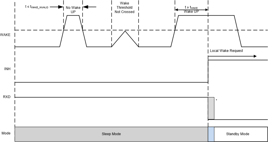
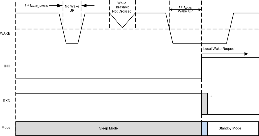
The WAKE terminal defaults to bi-directional input but can be configured for rising edge and falling edge transitions, see Figure 10-14 and Figure 10-15, by using WAKE_CONFIG register 11h[7:6]. Once the device enters sleep mode the WAKE terminal voltage level needs to be at either a low state or high state for tWAKE before a state transition for a WAKE input can be determined.
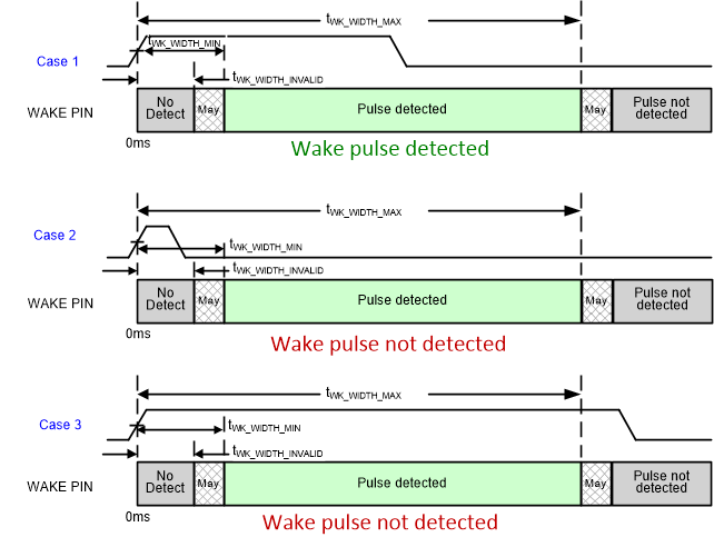
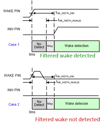
There are two other wake methods that can be utilized with the WAKE pin, a pulse wake and a filtered wake. For the pulsed wake input a pulse on the WAKE pin must be within a specified time to be considered valid. A pulse width less than tWAKE_INVALID will be filtered out for both the pulse and filtered wake configurations. For the pulse configuration, the pulse must be between tWK_WIDTH_MIN and tWK_WIDTH_MAX, see Figure 10-16. This figure provides three examples of pulses and whether the device will wake or not wake. tWK_WIDTH_MIN is determined by the value for tWK_WIDTH_INVALID which is set by register 11h[3:2]. There are two regions where a pulse may or may not be detected. By using register 1Bh[1], WAKE_WIDTH_MAX_DIS, the pulse mode can be configured as a filtered wake input. Writing a 1 to this bit will disable tWK_WIDTH_MAX and the WAKE input will be based upon the configuration of register 11h[3:2] which selects a tWK_WIDTH_INVALID and tWK_WIDTH_MIN value. A WAKE input of less than tWK_WIDTH_INVALID will be filtered out and if longer than tWK_WIDTH_MIN INH will turn on and device will enter standby mode. The region between the two may or may not be recognized, see Figure 10-17. Register 12h[7] determines the direction of the pulse or filter edge that is recognized. The status of the WAKE pin can be determined from register 11h[5:4]. When a WAKE pin change takes place, the device will register this as a rising edge or falling edge. This will be latched until a 00 is written to the bits.
The LWU circuitry is active in sleep mode, standby mode and transition state of going to sleep. If a valid LWU event occurs the device transitions to standby mode. The LWU circuitry is not active in normal mode. A constant high level on WAKE has an internal pull up to VSUP, and a constant low level on WAKE has an internal pull down to GND. On power up this may look like a LWU event and could be flagged as such.
 Figure 10-14 Local Wake Up – Rising Edge
 Figure 10-15 Local Wake Up – Falling Edge
When either a rising or falling edge is selected for the WAKE pin the state prior to the edge requires a tWAKE period of time.
- If a rising edge is selected and the device goes to sleep with WAKE high, a low of at least tWAKE must be present prior to the rising edge wake event
- If a falling edge is selected and the device goes to sleep with WAKE low, a high of at least tWAKE must be present prior to the falling edge wake event
- This requirement is not necessary for a bidirectional edge (default)
- Figure 10-14 and Figure 10-15 provide examples of a rising or falling edge WAKE input. tWAKE is based upon the time it takes from a valid WUP to INH turning on. RXD will be pulled low once VIO > UVIO and VCC > UVCC and standby mode is entered.
 Figure 10-16 WAKE Pin Pulse Behavior
 Figure 10-17 WAKE Pin Filtered Behavior