JAJSKV6D August 2020 – April 2024 DRV8714-Q1 , DRV8718-Q1
PRODMIX
- 1
- 1 特長
- 2 アプリケーション
- 3 概要
- 4 Device Comparison Table
- 5 Pin Configuration and Functions
- 6 Specifications
-
7 Detailed Description
- 7.1 Overview
- 7.2 Functional Block Diagram
- 7.3
Feature Description
- 7.3.1 External Components
- 7.3.2 Device Interface Variants
- 7.3.3 Input PWM Control Modes
- 7.3.4 Smart Gate Driver
- 7.3.5 Tripler (Dual-Stage) Charge Pump
- 7.3.6 Wide Common-Mode Current Shunt Amplifiers
- 7.3.7 Pin Diagrams
- 7.3.8
Protection and Diagnostics
- 7.3.8.1 Gate Driver Disable (DRVOFF/nFLT and EN_DRV)
- 7.3.8.2 Low IQ Powered Off Braking (POB, BRAKE)
- 7.3.8.3 Fault Reset (CLR_FLT)
- 7.3.8.4 DVDD Logic Supply Power on Reset (DVDD_POR)
- 7.3.8.5 PVDD Supply Undervoltage Monitor (PVDD_UV)
- 7.3.8.6 PVDD Supply Overvoltage Monitor (PVDD_OV)
- 7.3.8.7 VCP Charge Pump Undervoltage Lockout (VCP_UV)
- 7.3.8.8 MOSFET VDS Overcurrent Protection (VDS_OCP)
- 7.3.8.9 Gate Driver Fault (VGS_GDF)
- 7.3.8.10 Thermal Warning (OTW)
- 7.3.8.11 Thermal Shutdown (OTSD)
- 7.3.8.12 Offline Short Circuit and Open Load Detection (OOL and OSC)
- 7.3.8.13 Watchdog Timer
- 7.3.8.14 Fault Detection and Response Summary Table
- 7.4 Device Functional Modes
- 7.5 Programming
- 8 Register Maps
- 9 Application Implementation
- 10Device Documentation and Support
- 11Revision History
- 12Mechanical, Packaging, and Orderable Information
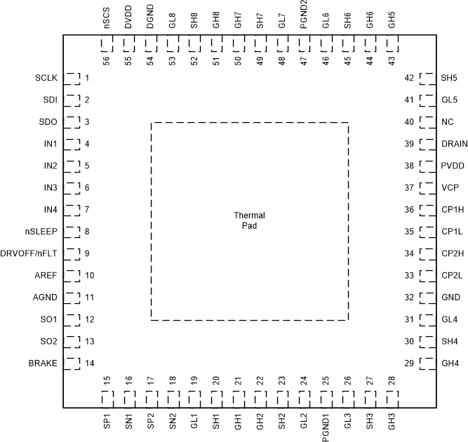
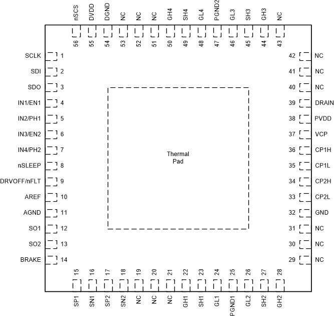
5.1 VQFN (RVJ) 56-Pin Package and Pin Functions
 Figure 5-1 DRV8718S-Q1 VQFN (RVJ) 56-Pin
Package Top View
 Figure 5-2 DRV8714S-Q1 VQFN (RVJ) 56-Pin
Package Top View
Figure 5-2 DRV8714S-Q1 VQFN (RVJ) 56-Pin
Package Top ViewTable 5-1 VQFN (RVJ) 56-Pin Package Pin Functions
| PIN | I/O | TYPE | DESCRIPTION | ||
|---|---|---|---|---|---|
| NO. | NAME | ||||
| DRV8718S-Q1 | DRV8714S-Q1 | ||||
| 1 | SCLK | I | Digital | Serial clock input. Serial data is shifted out and captured on the corresponding rising and falling edge on this pin. Internal pulldown resistor. | |
| 2 | SDI | I | Digital | Serial data input. Data is captured on the falling edge of the SCLK pin. Internal pulldown resistor. | |
| 3 | SDO | O | Digital | Serial data output. Data is shifted out on the rising edge of the SCLK pin. Push-pull output. | |
| 4 | IN1 | IN1/EN1 | I | Digital | Half-bridge and H-bridge control input. See Section 7.3.3. Internal pulldown. |
| 5 | IN2 | IN2/PH1 | I | Digital | |
| 6 | IN3 | IN3/EN2 | I | Digital | |
| 7 | IN4 | IN4/PH2 | I | Digital | |
| 8 | nSLEEP | I | Digital | Device enable pin. Logic low to shutdown the device and enter sleep mode. Internal pulldown resistor. | |
| 9 | DRVOFF/nFLT | I/O | Digital | Multi-function pin for either driver shutdown input or fault indicator output. See Section 7.3.8. Internal pulldown resistor. | |
| 10 | AREF | I | Power | External voltage reference and power supply for current sense amplifiers. Recommended to connect a 0.1µF, 6.3V ceramic capacitor between the AREF and AGND pins. | |
| 11 | AGND | I/O | Power | Device ground. Connect to system ground. | |
| 12 | SO1 | O | Analog | Shunt amplifier output. | |
| 13 | SO2 | O | Analog | Shunt amplifier output. | |
| 14 | BRAKE | I | Digital | Powered off braking pin. Logic high to enable low-side gate drivers while in low-power sleep mode. See Section 7.3.8.2. Internal pulldown resistor. | |
| 15 | SP1 | I | Analog | Amplifier positive input. Connect to positive terminal of the shunt resistor. | |
| 16 | SN1 | I | Analog | Amplifier negative input. Connect to negative terminal of the shunt resistor. | |
| 17 | SP2 | I | Analog | Amplifier positive input. Connect to positive terminal of the shunt resistor. | |
| 18 | SN2 | I | Analog | Amplifier negative input. Connect to negative terminal of the shunt resistor. | |
| 19 | GL1 | NC | O | Analog | Low-side gate driver output. Connect to the gate of the low-side MOSFET. |
| 20 | SH1 | NC | I | Analog | High-side source sense input. Connect to the high-side MOSFET source. |
| 21 | GH1 | NC | O | Analog | High-side gate driver output. Connect to the gate of the high-side MOSFET. |
| 22 | GH2 | GH1 | O | Analog | High-side gate driver output. Connect to the gate of the high-side MOSFET. |
| 23 | SH2 | SH1 | I | Analog | High-side source sense input. Connect to the high-side MOSFET source. |
| 24 | GL2 | GL1 | O | Analog | Low-side gate driver output. Connect to the gate of the low-side MOSFET. |
| 25 | PGND1 | I | Analog | Low-side MOSFET gate drive 1-4 sense and power return. Connect to system ground close to the device and half-bridge 1-4. | |
| 26 | GL3 | GL2 | O | Analog | Low-side gate driver output. Connect to the gate of the low-side MOSFET. |
| 27 | SH3 | SH2 | I | Analog | High-side source sense input. Connect to the high-side MOSFET source. |
| 28 | GH3 | GH2 | O | Analog | High-side gate driver output. Connect to the gate of the high-side MOSFET. |
| 29 | GH4 | NC | O | Analog | High-side gate driver output. Connect to the gate of the high-side MOSFET. |
| 30 | SH4 | NC | I | Analog | High-side source sense input. Connect to the high-side MOSFET source. |
| 31 | GL4 | NC | O | Analog | Low-side gate driver output. Connect to the gate of the low-side MOSFET. |
| 32 | GND | I/O | Ground | Device ground. Connect to system ground. | |
| 33 | CP2L | I/O | Power | Charge pump switching node. Connect a 100nF, PVDD-rated ceramic capacitor between the CP2H and CP2L pins. | |
| 34 | CP2H | I/O | Power | ||
| 35 | CP1L | I/O | Power | Charge pump switching node. Connect a 100nF, PVDD-rated ceramic capacitor between the CP1H and CP1L pins. | |
| 36 | CP1H | I/O | Power | ||
| 37 | VCP | I/O | Power | Charge pump output. Connect a 1µF, 16V ceramic capacitor between the VCP and PVDD pins. | |
| 38 | PVDD | I | Power | Device driver power supply input. Connect to the bridge power supply. Connect a 0.1µF, PVDD-rated ceramic capacitor and local bulk capacitance greater than or equal to 10µF between PVDD and GND pins. | |
| 39 | DRAIN | I | Analog | Bridge MOSFET drain voltage sense pin. Connect to common point of the high-side MOSFET drains. | |
| 40 | NC | — | — | No connection. | |
| 41 | GL5 | NC | O | Analog | Low-side gate driver output. Connect to the gate of the low-side MOSFET. |
| 42 | SH5 | NC | I | Analog | High-side source sense input. Connect to the high-side MOSFET source. |
| 43 | GH5 | NC | O | Analog | High-side gate driver output. Connect to the gate of the high-side MOSFET. |
| 44 | GH6 | GH3 | O | Analog | High-side gate driver output. Connect to the gate of the high-side MOSFET. |
| 45 | SH6 | SH3 | I | Analog | High-side source sense input. Connect to the high-side MOSFET source. |
| 46 | GL6 | GL3 | O | Analog | Low-side gate driver output. Connect to the gate of the low-side MOSFET. |
| 47 | PGND2 | I | Analog | Low-side MOSFET gate drive 5-8 sense and power return. Connect to system ground close to the device and half-bridge 5-8. | |
| 48 | GL7 | GL4 | O | Analog | Low-side gate driver output. Connect to the gate of the low-side MOSFET. |
| 49 | SH7 | SH4 | I | Analog | High-side source sense input. Connect to the high-side MOSFET source. |
| 50 | GH7 | GH4 | O | Analog | High-side gate driver output. Connect to the gate of the high-side MOSFET. |
| 51 | GH8 | NC | O | Analog | High-side gate driver output. Connect to the gate of the high-side MOSFET. |
| 52 | SH8 | NC | I | Analog | High-side source sense input. Connect to the high-side MOSFET source. |
| 53 | GL8 | NC | O | Analog | Low-side gate driver output. Connect to the gate of the low-side MOSFET. |
| 54 | DGND | I/O | Ground | Device ground. Connect to system ground. | |
| 55 | DVDD | I | Power | Device logic and digital output power supply input. Recommended to connect a 1.0µF, 6.3V ceramic capacitor between the DVDD and GND pins. | |
| 56 | nSCS | I | Digital | Serial chip select. A logic low on this pin enables serial interface communication. Internal pullup resistor. | |
Note: The DRV8718-Q1 56-Pin VQFN (RVJ)
and DRV8714-Q1 56-Pin VQFN (RVJ) packages are drop in pin-to-pin compatible. Please
note that the locations of half-bridges 1,2,3 and 4 are shifted for the DRV8714-Q1
to help with PCB routing.