JAJSL23B January 2021 – January 2022 TPS785-Q1
PRODUCTION DATA
- 1 特長
- 2 アプリケーション
- 3 概要
- 4 Revision History
- 5 Pin Configuration and Functions
- 6 Specifications
- 7 Detailed Description
-
8 Application and Implementation
- 8.1 Application Information
- 8.2 Typical Application
- 9 Power Supply Recommendations
- 10Layout
- 11Device and Documentation Support
- 12Mechanical, Packaging, and Orderable Information
7.3.1 Foldback Current Limit
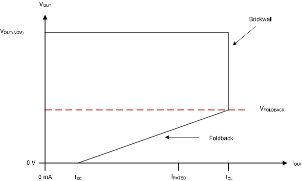
The device has an internal current limit circuit that protects the regulator during transient high-load current faults or shorting events. The current limit is a hybrid brickwall-foldback scheme. The current limit transitions from a brickwall scheme to a foldback scheme at the foldback voltage (VFOLDBACK). In a high-load current fault with the output voltage above VFOLDBACK, the brickwall scheme limits the output current to the current limit (ICL). When the voltage drops below VFOLDBACK, a foldback current limit activates that scales back the current as the output voltage approaches GND. When the output is shorted, the device supplies a typical current called the short-circuit current limit (ISC). ICL and ISC are listed in the Electrical Characteristics table.
For this device, VFOLDBACK = 0.4 × VOUT(NOM).
The output voltage is not regulated when the device is in current limit. When a current limit event occurs, the device begins to heat up because of the increase in power dissipation. When the device is in brickwall current limit, the pass transistor dissipates power [(VIN – VOUT) × ICL]. When the device output is shorted and the output is below VFOLDBACK, the pass transistor dissipates power [(VIN – VOUT) × ISC]. If thermal shutdown is triggered, the device turns off. After the device cools down, the internal thermal shutdown circuit turns the device back on. If the output current fault condition continues, the device cycles between current limit and thermal shutdown. For more information on current limits, see the Know Your Limits application report.
Figure 7-3 shows a diagram of the foldback current limit.
 Figure 7-3 Foldback Current Limit