JAJSL78D september   2009  – may 2021 BQ24050 , BQ24052

PRODUCTION DATA  

  1.   1
  2. 特長
  3. アプリケーション
  4. 概要
  5. Revision History
  6. Pin Configuration and Functions
  7. Specifications
    1. 6.1 Absolute Maximum Ratings #GUID-2D40D94D-8E9B-4250-B39D-57145C9518DB/SLUS9405873
    2. 6.2 ESD Ratings
    3. 6.3 Recommended Operating Conditions #GUID-C5354C38-DF78-4F74-91ED-68706C55D3F9/SLUS9401392
    4. 6.4 Thermal Information
    5. 6.5 Electrical Characteristics
    6. 6.6 Timing Requirements
    7. 6.7 Switching Characteristics
    8. 6.8 Typical Characteristics
      1. 6.8.1 Power Up, Down, OVP, Disable and Enable Waveforms
      2. 6.8.2 Protection Circuits Waveforms
  8. Detailed Description
    1. 7.1 Overview
    2. 7.2 Functional Block Diagram
    3. 7.3 Feature Description
      1. 7.3.1  Power Down, or Undervoltage Lockout (UVLO)
      2. 7.3.2  Power Up
      3. 7.3.3  D+, D– Detection
      4. 7.3.4  New Charge Cycle
      5. 7.3.5  Overvoltage Protection (OVP) – Continuously Monitored
      6. 7.3.6  CHG Pin Indication
      7. 7.3.7  CHG LED Pullup Source
      8. 7.3.8  Input DPM Mode (VIN-DPM or IN-DPM)
      9. 7.3.9  OUT
      10. 7.3.10 ISET
      11. 7.3.11 TS
      12. 7.3.12 Termination and Timer Disable Mode (TTDM) -TS Pin High
      13. 7.3.13 Timers
      14. 7.3.14 Termination
      15. 7.3.15 Battery Detect Routine
      16. 7.3.16 Refresh Threshold
      17. 7.3.17 Starting a Charge on a Full Battery
    4. 7.4 Device Functional Modes
      1. 7.4.1 Sleep Mode
    5. 7.5 Programming
      1. 7.5.1 PRE_TERM – Precharge and Termination Programmable Threshold
      2. 7.5.2 ISET2
  9. Application and Implementation
    1. 8.1 Application Information
    2. 8.2 Typical Applications
      1. 8.2.1 BQ2405x Charger Application Design Example
        1. 8.2.1.1 Design Requirements
        2. 8.2.1.2 Detailed Design Procedure
          1. 8.2.1.2.1 Program the Fast Charge Current, ISET
          2. 8.2.1.2.2 Program the Termination Current Threshold, ITERM
          3. 8.2.1.2.3 TS Function
          4. 8.2.1.2.4 CHG
          5. 8.2.1.2.5 Selecting IN and OUT Pin Capacitors
        3. 8.2.1.3 Application Curves
  10. Power Supply Recommendations
  11. 10Layout
    1. 10.1 Layout Guidelines
    2. 10.2 Layout Example
    3. 10.3 Thermal Considerations
      1. 10.3.1 Leakage Current Effects on Battery Capacity
  12. 11Device and Documentation Support
    1. 11.1 Device Support
      1. 11.1.1 サード・パーティ製品に関する免責事項
    2. 11.2 Documentation Support
      1. 11.2.1 Related Documentation
    3. 11.3 ドキュメントの更新通知を受け取る方法
    4. 11.4 サポート・リソース
    5. 11.5 Trademarks
    6. 11.6 静電気放電に関する注意事項
    7. 11.7 用語集
  13.   Mechanical, Packaging, and Orderable Information

Protection Circuits Waveforms

GUID-B1FFCA0C-438E-4400-A89F-59AE627567DF-low.gif
CH4: IOUT (0.2 A/Div)
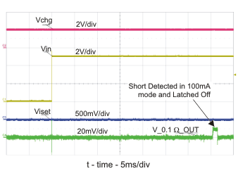
Figure 6-8 ISET Shorted Before USB Power Up
GUID-A293685E-7C38-434B-BA4F-91840A5DCAE0-low.gif
Figure 6-10 DPM – USB Current Limits – VIN Regulated to 4.4 V
GUID-EF9DFA87-0763-47EB-9229-20B3F7480671-low.gif
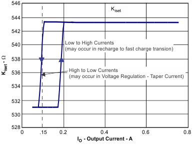
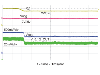
Figure 6-12 KISET for Low and High Currents
GUID-3BD4E29B-CC84-4525-BD48-93CC6ABC54C3-low.gif
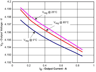
Figure 6-14 Load Regulation Overtemperature
GUID-86A35D85-C2B0-4D70-84E1-01F30A6BD9A6-low.gif
CH4: IOUT (0.2 A/Div)
Figure 6-9 DPM – Adaptor Current Limits – VIN Regulated to 4.3 V
GUID-4839605D-D518-4913-AA07-C9F9243E408E-low.gif
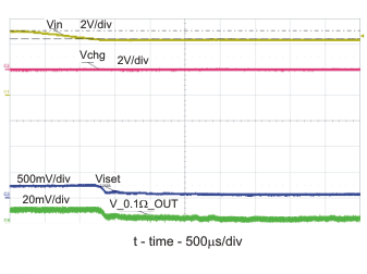
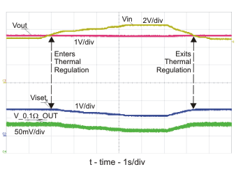
The IC temperature rises to 125°C and enters thermal regulation. Charge current is reduced to regulate the IC at 125°C .
VIN is reduced, the IC temperature drops, the charge current returns to the programmed value.
Figure 6-11 Thermal Regulator – VIN Increases
GUID-B2F35EBD-3EE7-4B62-BC03-F6B5D9FF5CF6-low.gif
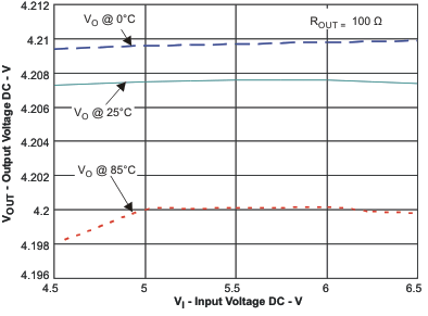
Figure 6-13 Line Regulation
GUID-4C12D568-37E7-461E-A078-CB139F92B5D4-low.gif
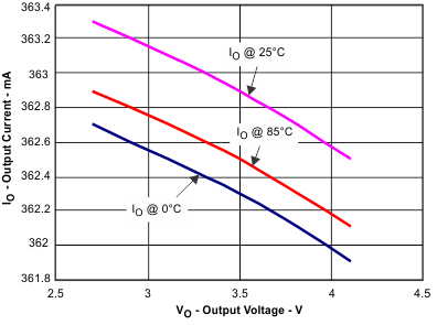
Figure 6-15 Current Regulation Overtemperature