JAJSL87H january 2010 – april 2021 BQ24090 , BQ24091 , BQ24092 , BQ24093 , BQ24095
PRODUCTION DATA
- 1
- 1 特長
- 2 アプリケーション
- 3 概要
- 4 Revision History
- 5 概要 (続き)
- 6 Device Options
- 7 Pin Configuration and Functions
-
8 Specifications
- 8.1 Absolute Maximum Ratings #GUID-9FC6FB05-10A6-4323-9A52-EE32AE4C5F67/SLUS9405873
- 8.2 ESD Ratings
- 8.3 Recommended Operating Conditions #GUID-4D70561B-CB71-403D-B731-8EF5DEBEBDF9/SLUS9401392
- 8.4 Thermal Information
- 8.5 Dissipation Ratings #GUID-196940BE-C3C2-4CDF-A8A4-7C186292F803/SLUS9404025 #GUID-196940BE-C3C2-4CDF-A8A4-7C186292F803/SLUS9403553
- 8.6 Electrical Characteristics
- 8.7 Typical Characteristics
-
9 Detailed Description
- 9.1 Overview
- 9.2 Functional Block Diagram
- 9.3
Feature Description
- 9.3.1 Power Down or Undervoltage Lockout (UVLO)
- 9.3.2 UVLO
- 9.3.3 Power Up
- 9.3.4 Sleep Mode
- 9.3.5 New Charge Cycle
- 9.3.6 Overvoltage Protection (OVP) – Continuously Monitored
- 9.3.7 Power Good Indication ( PG)
- 9.3.8 CHG Pin Indication
- 9.3.9 CHG and PG LED Pullup Source
- 9.3.10 IN-DPM (VIN-DPM or IN–DPM)
- 9.3.11 OUT
- 9.3.12 ISET
- 9.3.13 PRE_TERM – Precharge and Termination Programmable Threshold
- 9.3.14 ISET2
- 9.3.15 TS
- 9.4 Device Functional Modes
- 10Application and Implementation
- 11Power Supply Recommendations
- 12Layout
- 13Device and Documentation Support
- Mechanical, Packaging, and Orderable Information
7 Pin Configuration and Functions
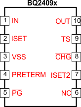
 Figure 7-1 DGQ Package10 PinsTop View
Table 7-1 Pin Functions
| PIN | I/O | DESCRIPTION | |
|---|---|---|---|
| NAME | NO. | ||
| CHG | 8 | O | Low (FET on) indicates charging and Open Drain (FET off) indicates no charging or charge complete. |
| IN | 1 | I | Input power, connected to external DC supply (AC adapter or USB port). Expected range of bypass capacitors 1 μF to 10 μF, connect from IN to VSS. |
| ISET | 2 | I | Programs the fast-charge current setting. External resistor from ISET to VSS defines fast charge current value. Range is 10.8 kΩ (50 mA) to 540 Ω (1000 mA). |
| ISET2 | 7 | I | Programming the input/output current limit for the USB or adaptor
source: high = 500 mA max, low = ISET, FLOAT = 100 mA max. |
| NC | 6 | NA | Do not make a connection to this pin (for internal use) – do not route through this pin. |
| OUT | 10 | O | Battery connection. System load may be connected. Average load should not be excessive, allowing battery to charge within the 10 hour safety timer window. Expected range of bypass capacitors 1 μF to 10 μF. |
| PG | 5 | O | Low (FET on) indicates the input voltage is above UVLO and the OUT (battery) voltage. |
| PRE-TERM | 4 | I | Programs the current termination threshold (5 to 50% of Iout
which is set by ISET) and sets the pre-charge current to twice the
termination current level. Expected range of programming resistor is 1 kΩ to 10 kΩ (2k: Ipgm/10 for term; Ipgm/5 for precharge). |
| TS | 9 | I | Temperature sense pin connected to BQ24090/2/5 -10k at 25°C NTC thermistor and BQ24091/3 -100 k at 25°C NTC thermistor, in the battery pack. Floating TS pin or pulling high puts part in TTDM Charger Mode and disable TS monitoring, timers and termination. Pulling pin low disables the IC. If NTC sensing is not needed, connect this pin to VSS through an external 10-kΩ/100-kΩ resistor. A 250 kΩ from TS to ground will prevent IC entering TTDM mode when battery with thermistor is removed. |
| VSS | 3 | – | Ground terminal |
| Thermal Pad and Package | — | — | There is an internal electrical connection between the exposed thermal pad and the VSS pin of the device. The thermal pad must be connected to the same potential as the VSS pin on the printed circuit board. Do not use the thermal pad as the primary ground input for the device. VSS pin must be connected to ground at all times. |