JAJSL87H january 2010 – april 2021 BQ24090 , BQ24091 , BQ24092 , BQ24093 , BQ24095
PRODUCTION DATA
- 1
- 1 特長
- 2 アプリケーション
- 3 概要
- 4 Revision History
- 5 概要 (続き)
- 6 Device Options
- 7 Pin Configuration and Functions
-
8 Specifications
- 8.1 Absolute Maximum Ratings #GUID-9FC6FB05-10A6-4323-9A52-EE32AE4C5F67/SLUS9405873
- 8.2 ESD Ratings
- 8.3 Recommended Operating Conditions #GUID-4D70561B-CB71-403D-B731-8EF5DEBEBDF9/SLUS9401392
- 8.4 Thermal Information
- 8.5 Dissipation Ratings #GUID-196940BE-C3C2-4CDF-A8A4-7C186292F803/SLUS9404025 #GUID-196940BE-C3C2-4CDF-A8A4-7C186292F803/SLUS9403553
- 8.6 Electrical Characteristics
- 8.7 Typical Characteristics
-
9 Detailed Description
- 9.1 Overview
- 9.2 Functional Block Diagram
- 9.3
Feature Description
- 9.3.1 Power Down or Undervoltage Lockout (UVLO)
- 9.3.2 UVLO
- 9.3.3 Power Up
- 9.3.4 Sleep Mode
- 9.3.5 New Charge Cycle
- 9.3.6 Overvoltage Protection (OVP) – Continuously Monitored
- 9.3.7 Power Good Indication ( PG)
- 9.3.8 CHG Pin Indication
- 9.3.9 CHG and PG LED Pullup Source
- 9.3.10 IN-DPM (VIN-DPM or IN–DPM)
- 9.3.11 OUT
- 9.3.12 ISET
- 9.3.13 PRE_TERM – Precharge and Termination Programmable Threshold
- 9.3.14 ISET2
- 9.3.15 TS
- 9.4 Device Functional Modes
- 10Application and Implementation
- 11Power Supply Recommendations
- 12Layout
- 13Device and Documentation Support
- Mechanical, Packaging, and Orderable Information
9.3.5 New Charge Cycle
A new charge cycle is started when a good power source is applied, performing a chip disable/enable (TS pin), exiting Termination and Timer Disable Mode (TTDM), detecting a battery insertion or the OUT voltage dropping below the VRCH threshold. The CHG pin is active low only during the first charge cycle, therefore exiting TTDM or a dropping below VRCH will not turn on the CHG pin FET, if the CHG pin is already high impedance.
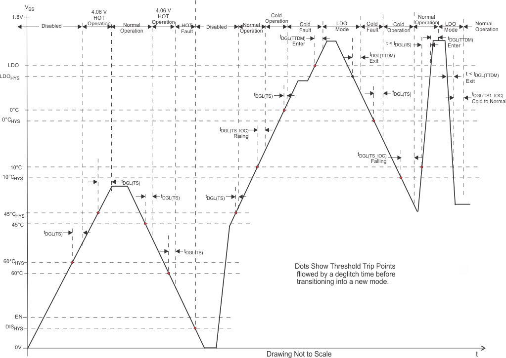
 Figure 9-2 TS Battery Temperature Bias Threshold and Deglitch Timers
 Figure 9-3 BQ2409x Power-Up Flow
Diagram