JAJSLF9B December 2015 – March 2021 LMR16030
PRODUCTION DATA
- 1 特長
- 2 アプリケーション
- 3 概要
- 4 Revision History
- 5 Pin Configuration and Functions
- 6 Specifications
-
7 Detailed Description
- 7.1 Overview
- 7.2 Functional Block Diagram
- 7.3
Feature Description
- 7.3.1 Fixed Frequency Peak Current Mode Control
- 7.3.2 Slope Compensation
- 7.3.3 Sleep Mode
- 7.3.4 Low Dropout Operation and Bootstrap Voltage (BOOT)
- 7.3.5 Adjustable Output Voltage
- 7.3.6 Enable and Adjustable Undervoltage Lockout
- 7.3.7 External Soft Start
- 7.3.8 Switching Frequency and Synchronization (RT/SYNC)
- 7.3.9 Power Good (PGOOD)
- 7.3.10 Overcurrent and Short Circuit Protection
- 7.3.11 Overvoltage Protection
- 7.3.12 Thermal Shutdown
- 7.4 Device Functional Modes
- 8 Application and Implementation
- 9 Power Supply Recommendations
- 10Layout
- 11Device and Documentation Support
- 12Mechanical, Packaging, and Orderable Information
7.3.1 Fixed Frequency Peak Current Mode Control
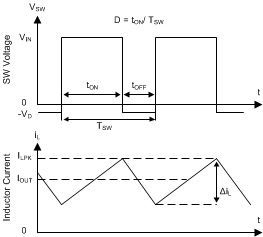
The following operating description of the LMR16030 will refer to the Functional Block Diagram and to the waveforms in Figure 7-1. The LMR16030 output voltage is regulated by turning on the high-side N-MOSFET with controlled ON time. During high-side switch ON time, the SW pin voltage swings up to approximately VIN, and the inductor current iL increases with alinear slope (VIN – VOUT) / L. When the high-side switch is off, inductor current discharges through a freewheel diode with a slope of –VOUT / L. The control parameter of the buck converter is defined as Duty Cycle D = tON / TSW, where tON is the high-side switch ON time and TSW is the switching period. The regulator control loop maintains a constant output voltage by adjusting the duty cycle D. In an ideal buck converter where losses are ignored, D is proportional to the output voltage and inversely proportional to the input voltage: D = VOUT / VIN.
 Figure 7-1 SW Node and Inductor Current Waveforms in Continuous Conduction Mode (CCM)
The LMR16030 employs fixed-frequency peak current mode control. A voltage feedback loop is used to get accurate DC voltage regulation by adjusting the peak current command based on voltage offset. The peak inductor current is sensed from the high-side switch and compared to the peak current to control the ON time of the high-side switch. The voltage feedback loop is internally compensated, which allows for fewer external components, makes it easy to design, and provides stable operation with almost any combination of output capacitors. The regulator operates with fixed switching frequency at normal load condition. At very light load, the LMR16030 operates in sleep mode to maintain high efficiency and the switching frequency decreases with reduced load current.