JAJSLI4A May   2021  – December 2021 ISOW1044

PRODUCTION DATA  

  1. 特長
  2. アプリケーション
  3. 概要
  4. Revision History
  5. 概要 (続き)
  6. Device Comparison Table
  7. Pin Configuration and Functions
  8. Specifications
    1. 8.1  Absolute Maximum Ratings
    2. 8.2  ESD Ratings
    3. 8.3  Recommended Operating Conditions
    4. 8.4  ThermalInformation
    5. 8.5  Power Ratings
    6. 8.6  Insulation Specifications
    7. 8.7  Safety-Related Certifications
    8. 8.8  Safety Limiting Values
    9. 8.9  Electrical Characteristics
    10. 8.10 Supply Current Characteristics
    11. 8.11 Switching Characteristics
    12. 8.12 Insulation Characteristics Curves
    13. 8.13 Typical Characteristics
  9. Parameter Measurement Information
  10. 10Detailed Description
    1. 10.1 Overview
    2. 10.2 Power Isolation
    3. 10.3 Signal Isolation
    4. 10.4 CAN Transceiver
      1. 10.4.1 Remote Wake Request via Wake-Up Pattern (WUP) in Standby Mode
    5. 10.5 Functional Block Diagram
    6. 10.6 Feature Description
      1. 10.6.1 CAN Bus States
      2. 10.6.2 Digital Inputs and Outputs: TXD (Input) and RXD (Output)
      3. 10.6.3 TXD Dominant Timeout (DTO)
      4. 10.6.4 Power-Up and Power-Down Behavior
      5. 10.6.5 Protection Features
      6. 10.6.6 Floating Pins, Unpowered Device
      7. 10.6.7 Glitch-Free Power Up and Power Down
    7. 10.7 Device Functional Modes
    8. 10.8 Device I/O Schematics
  11. 11Application and Implementation
    1. 11.1 Application Information
    2. 11.2 Typical Application
      1. 11.2.1 Design Requirements
      2. 11.2.2 Detailed Design Procedure
        1. 11.2.2.1 Bus Loading, Length and Number of Nodes
        2. 11.2.2.2 CAN Termination
      3. 11.2.3 Application Curve
      4. 11.2.4 Insulation Lifetime
  12. 12Power Supply Recommendations
  13. 13Layout
    1. 13.1 Layout Guidelines
    2. 13.2 Layout Example
  14. 14Device and Documentation Support
    1. 14.1 Documentation Support
      1. 14.1.1 Related Documentation
    2. 14.2 Receiving Notification of Documentation Updates
    3. 14.3 サポート・リソース
    4. 14.4 Trademarks
    5. 14.5 静電気放電に関する注意事項
    6. 14.6 用語集
  15. 15Mechanical, Packaging, and Orderable Information

Typical Characteristics

VDD = VIO , VISOIN = VISOOUT, CL(RXD) = 15 pF , RL = 60 Ω, TA = 25°C unless otherwise noted.

GUID-20211121-SS0I-VJQJ-WD1W-HQMMSV6MDKBM-low.svg
VISOOUT = 5 V STB = Low
Figure 8-3 VDD Supply Current vs Datarate
GUID-20211121-SS0I-7RK8-QN8Q-MCHD7HM7GZM4-low.svg
VISOOUT = 5 V STB = Low
Figure 8-5 VIO Supply Current vs Datarate
GUID-20211121-SS0I-LRHG-6RRZ-QHKWXRZWFSWS-low.svg
VDD = 5 V STB = Low VISOOUT = 5 V
Figure 8-7 VIOI Non-standby Current vs Temperature
GUID-20211121-SS0I-LXB1-J9B3-RCXG4XHD7MHW-low.svg
VDD = 5 V STB = Low VISOOUT = 5 V
CL = 100 pF
Figure 8-9 Loop Delay (Dominant to Recessive) vs Temperature
GUID-20211121-SS0I-NNFP-6SGP-VXVSMHBFG9NM-low.svg
VDD = 5 V STB = Low
Figure 8-11 Receiver differential threshold voltage vs Temperature
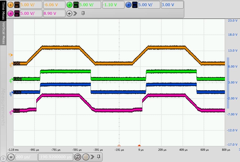
GUID-20211122-SS0I-R2F2-KHLH-FBJXLP4J2GDV-low.jpg
Figure 8-13 Glitch Free Power Up on VDD
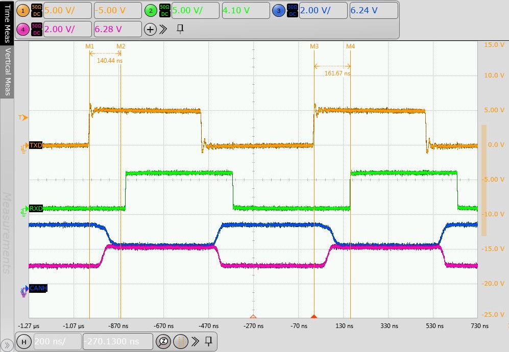
GUID-20211121-SS0I-R3SV-ZBPP-QTBJR4T4V9HG-low.jpg
Figure 8-15 Typical TXD, RXD, CANH and CANL Waveforms at 2 Mbps
GUID-20211121-SS0I-TXVB-7KHN-MNCXQ3QRZWQ2-low.svg
VDD = 5 V STB = Low VISOOUT = 5 V
Figure 8-4 VDD Supply Current vs Temperature
GUID-20211121-SS0I-HQDM-WPXS-KBBV7BMKTVML-low.svg
VDD = 5 V STB = High VISOOUT = 5 V
Figure 8-6 VIO Standby Current vs Temerature
GUID-20211121-SS0I-3M1M-JVW4-JXJBTBK00SLC-low.svg
VDD = 5 V STB = Low VISOOUT = 5 V
CL = 100 pF
Figure 8-8 Loop Delay (Recessive to Dominant) vs Temperature
GUID-20211121-SS0I-XR03-NZV4-XZKPQZGBF8D9-low.svg
VDD = 5 V STB = Low
Figure 8-10 Dominant state differential output voltage vs Temperature
GUID-20211121-SS0I-LVMC-4ZWP-QZDDRPH0QW2R-low.svg
VDD = 5 V STB = Low
Figure 8-12 Dominant Timeout vs Temperature
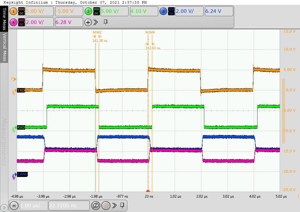
GUID-20211121-SS0I-SBZ9-9GV8-B33FJLLHRSTT-low.jpg
Figure 8-14 Typical TXD, RXD, CANH and CANL Waveforms at 500 kbps
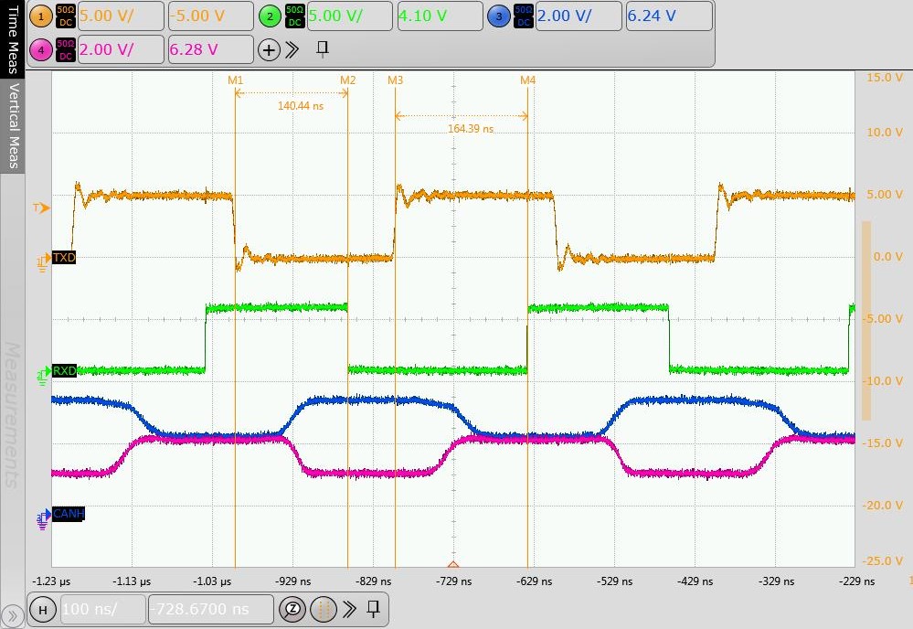
GUID-20211122-SS0I-GSJL-SL81-1XFKS9QTJ8BK-low.jpg
Figure 8-16 Typical TXD, RXD, CANH and CANL Waveforms at 5 Mbps