JAJSLJ8 March 2021 TPSM13604H
PRODUCTION DATA
- 1 特長
- 2 アプリケーション
- 3 概要
- 4 Revision History
- 5 Pin Configuration and Functions
- 6 Specifications
- 7 Detailed Description
-
8 Application and Implementation
- 8.1 Application Information
- 8.2
Typical Application
- 8.2.1 Design Requirements
- 8.2.2
Detailed Design Procedure
- 8.2.2.1 Design Steps for the TPSM13604 Application
- 8.2.3 Application Curve
- 9 Power Supply Recommendations
- 10Layout
- 11Device and Documentation Support
- 12Mechanical, Packaging, and Orderable Information
10.2.1 Power Dissipation and Board Thermal Requirements
For a design case of VIN = 12 V, VOUT = 9.5 V, IOUT = 4 A, TA (MAX) = 50°C , TJUNCTION = 125°C, and continuous operation, the device must see a maximum junction-to-ambient thermal resistance of:
This RθJA-MAX ensures that the junction temperature of the regulator under continuous operation does not exceed TJ-MAX in the particular application ambient temperature.
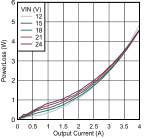
To calculate the required RθJA-MAX, you need to get an estimate for the power losses in the IC. Figure 10-4 is taken form the Typical Characteristics and shows the power dissipation of the TPSM13604 for VOUT = 9.5 V.
 Figure 10-4 Power Dissipation VOUT = 9.5 V
Using the 50°C TA power dissipation data as a conservative starting point, the power dissipation PD for VIN = 12 V and VOUT = 9.5 V is estimated to be 4.85 W under continuous operation. The necessary RθJA-MAX can now be calculated.
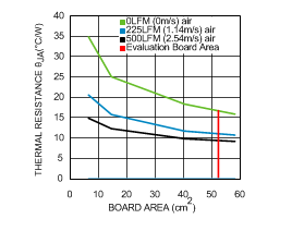
To achieve this thermal resistance, the PCB is required to dissipate the heat effectively. The area of the PCB has a direct effect on the overall junction-to-ambient thermal resistance. To estimate the necessary copper area, refer to Figure 10-5. This graph is taken from the Section 6.6 (Figure 6-12) and shows how the RθJA varies with the PCB area.
 Figure 10-5 Package Thermal
Resistance RθJA 4-Layer PCB with 1-oz Copper
Figure 10-5 Package Thermal
Resistance RθJA 4-Layer PCB with 1-oz CopperFor RθJA-MAX < 15.5°C/W and only natural convection (that is, no air flow), the PCB area must be at least 52 cm2. This corresponds to a square board with 7.25-cm × 7.25-cm (2.85 in x 2.85 in) copper area, four layers, and 1-oz copper thickness. Higher copper thickness further improves the overall thermal performance. As a reference, the evaluation board has 2-oz copper on the top and bottom layers, achieving RθJA of 14.9°C/W for the same board area. Note thermal vias must be placed under the IC package to easily transfer heat from the top layer of the PCB to the inner layers and the bottom layer. For more guidelines and insight on PCB copper area, thermal vias placement, and general thermal design practices, see the application note AN-2020 Thermal Design By Insight, Not Hindsight.