JAJSLK0B march   2021  – june 2023 TMUX7462F

PRODUCTION DATA  

  1.   1
  2. 特長
  3. アプリケーション
  4. 概要
  5. Revision History
  6. Pin Configuration and Functions
  7. Specifications
    1. 6.1  Absolute Maximum Ratings
    2. 6.2  ESD Ratings
    3. 6.3  Thermal Information
    4. 6.4  Recommended Operating Conditions
    5. 6.5  Electrical Characteristics (Global)
    6. 6.6  ±15 V Dual Supply: Electrical Characteristics
    7. 6.7  ±20 V Dual Supply: Electrical Characteristics
    8. 6.8  12 V Single Supply: Electrical Characteristics
    9. 6.9  36 V Single Supply: Electrical Characteristics
    10. 6.10 Typical Characteristics
  8. Parameter Measurement Information
    1. 7.1  On-Resistance
    2. 7.2  On-Leakage Current
    3. 7.3  Input and Output Leakage Current under Overvoltage Fault
    4. 7.4  Fault Response Time
    5. 7.5  Fault Recovery Time
    6. 7.6  Fault Flag Response Time
    7. 7.7  Fault Flag Recovery Time
    8. 7.8  Fault Drain Enable Time
    9. 7.9  Inter-Channel Crosstalk
    10. 7.10 Bandwidth
    11. 7.11 THD + Noise
  9. Detailed Description
    1. 8.1 Overview
    2. 8.2 Functional Block Diagram
    3. 8.3 Feature Description
      1. 8.3.1 Flat ON-Resistance
      2. 8.3.2 Protection Features
        1. 8.3.2.1 Input Voltage Tolerance
        2. 8.3.2.2 Powered-Off Protection
        3. 8.3.2.3 Fail-Safe Logic
        4. 8.3.2.4 Overvoltage Protection and Detection
        5. 8.3.2.5 Latch-Up Immunity
        6. 8.3.2.6 EMC Protection
      3. 8.3.3 Overvoltage Fault Flags
      4. 8.3.4 Bidirectional Operation
    4. 8.4 Device Functional Modes
      1. 8.4.1 Normal Mode
      2. 8.4.2 Fault Mode
      3. 8.4.3 Truth Table
  10. Application and Implementation
    1. 9.1 Application Information
    2. 9.2 Typical Application
      1. 9.2.1 Design Requirements
      2. 9.2.2 Detailed Design Procedure
      3. 9.2.3 Application Curves
    3. 9.3 Power Supply Recommendations
    4. 9.4 Layout
      1. 9.4.1 Layout Guidelines
      2. 9.4.2 Layout Example
  11. 10Device and Documentation Support
    1. 10.1 Documentation Support
      1. 10.1.1 Related Documentation
    2. 10.2 ドキュメントの更新通知を受け取る方法
    3. 10.3 サポート・リソース
    4. 10.4 Trademarks
    5. 10.5 静電気放電に関する注意事項
    6. 10.6 用語集
  12. 11Mechanical, Packaging, and Orderable Information

On-Resistance

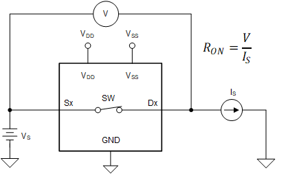
The TMUX7462F's on-resistance is the ohmic resistance across the source (Sx) and drain (Dx) pins of the device. The on-resistance varies with input voltage and supply voltage. The symbol RON is used to denote on-resistance. The measurement setup used to measure RON is shown in Figure 7-1. ΔRON represents the difference between the RON of any two channels, while RON_FLAT denotes the flatness that is defined as the difference between the maximum and minimum value of on-resistance measured over the specified analog signal range.
GUID-20211018-SS0I-JM81-WQ1Z-LZX1XN1J9MLW-low.gifFigure 7-1 On-Resistance Measurement Setup