JAJSLO9D June   2015  – May 2021 LM53600-Q1 , LM53601-Q1

PRODUCTION DATA  

  1. 特長
  2. アプリケーション
  3. 概要
  4. Revision History
  5. Device Comparison
  6. Pin Configuration and Functions
  7. Specifications
    1. 7.1 Absolute Maximum Ratings
    2. 7.2 ESD Ratings
    3. 7.3 Recommended Operating Conditions
    4. 7.4 Thermal Information
    5. 7.5 Electrical Characteristics
    6. 7.6 System Characteristics
    7. 7.7 Timing Requirements
    8. 7.8 Typical Characteristics
  8. Detailed Description
    1. 8.1 Overview
    2. 8.2 Functional Block Diagram
    3. 8.3 Feature Description
      1. 8.3.1 Control Scheme
      2. 8.3.2 Soft-Start Function
      3. 8.3.3 Current Limit
      4. 8.3.4 Hiccup Mode
      5. 8.3.5 RESET Function
      6. 8.3.6 Forced PWM Operation
      7. 8.3.7 Auto Mode Operation and IQ_VIN
      8. 8.3.8 SYNC Operation
      9. 8.3.9 Spread Spectrum
    4. 8.4 Device Functional Modes
      1. 8.4.1 Shutdown
      2. 8.4.2 FPWM Operation
      3. 8.4.3 Auto Mode Operation
  9. Applications and Implementation
    1. 9.1 Application Information
    2. 9.2 Typical Applications
      1. 9.2.1 Off-Battery 5-V, 1-A Output Automotive Converter with Spread Spectrum
        1. 9.2.1.1 Design Requirements
        2. 9.2.1.2 Detailed Design Procedure
          1. 9.2.1.2.1 Inductor Selection
          2. 9.2.1.2.2 Output Capacitor Selection
          3. 9.2.1.2.3 Input Capacitor Selection
          4. 9.2.1.2.4 FB Voltage Divider for Adjustable Versions
          5. 9.2.1.2.5 RPU - RESET Pull Up Resistor
        3. 9.2.1.3 Application Curves
      2. 9.2.2 Off-Battery 3.3 V, 1 A Output Automotive Converter with Spread Spectrum
        1. 9.2.2.1 Design Requirements
        2. 9.2.2.2 Design Procedure
        3. 9.2.2.3 Application Curves
    3. 9.3 Do's and Don't's
  10. 10Power Supply Recommendations
  11. 11Layout
    1. 11.1 Layout Guidelines
      1. 11.1.1 Ground and Thermal Plane Considerations
    2. 11.2 Layout Example
  12. 12Device and Documentation Support
    1. 12.1 Documentation Support
      1. 12.1.1 Related Documentation
    2. 12.2 Receiving Notification of Documentation Updates
    3. 12.3 サポート・リソース
    4. 12.4 Trademarks
    5. 12.5 静電気放電に関する注意事項
    6. 12.6 用語集
  13. 13Mechanical, Packaging, and Orderable Information

Current Limit

The LM53600-Q1 and LM53601-Q1 devices use two current limits which allow the use of smaller inductors than systems utilizing a single current limit. A coarse high side or peak current limit is provided to protect against faults and saturated inductors. High side current limit limits the duration of high sides FET's on period during a given clock cycle. A precision valley current limit prevents excessive average output current from the Buck converter of the LM53600-Q1 and LM53601-Q1 devices. A new switching cycle is not initiated until inductor current drops below the valley current limit. This scheme allows use of inductors with saturation current rated less than twice the rated operating current of the LM53600-Q1 or LM53601-Q1.
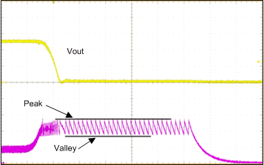
GUID-4C4DBB2D-1D67-4B7D-B24D-4914C0062DD8-low.gifFigure 8-3 Current Limit Operation

Figure 8-3 shows the response of the LM53600-Q1 or LM53601-Q1 device to a short circuit: Peak current limit prevents excessive peak current while valley current limit prevents excessive average inductor current. After a small number of cycles, hiccup mode is activated.