JAJSLO9D June 2015 – May 2021 LM53600-Q1 , LM53601-Q1
PRODUCTION DATA
- 1 特長
- 2 アプリケーション
- 3 概要
- 4 Revision History
- 5 Device Comparison
- 6 Pin Configuration and Functions
- 7 Specifications
- 8 Detailed Description
- 9 Applications and Implementation
- 10Power Supply Recommendations
- 11Layout
- 12Device and Documentation Support
- 13Mechanical, Packaging, and Orderable Information
6 Pin Configuration and Functions
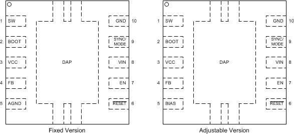
 Figure 6-1 DSX Package10-Pin WSONTop View
Table 6-1 Pin Functions
| PIN | TYPE(1) | DESCRIPTION | |
|---|---|---|---|
| NO. | NAME | ||
| 1 | SW | P | Regulator switch node. Connect to output inductor. |
| 2 | BOOT | I | High side gate driver upper supply rail. Connect a 100-nF capacitor from SW pin to BOOT. An internal diode charges the capacitor while SW node is low. |
| 3 | VCC | P | Internal 3-V regulator output. Used as supply to internal control circuits. Connect a high quality 1.0-μF capacitor from this pin to AGND for fixed versions or to GND for adjustable versions. |
| 4 | FB (Fixed Versions) | I/P | Fixed version only, this pin serves as feedback for output voltage as well as power source for VCC’s regulator. Connect to output node. Place 10-nF bypass capacitor immediately adjacent to this pin. |
| FB (ADJ Version) | I | ADJ version only, this pin serves as feedback for output voltage only. Connect to output through a voltage divider which determines output voltage set point. | |
| 5 | AGND (Fixed Version) | G | Fixed versions only, this is the ground to which input signals and FB are compared. |
| BIAS (ADJ Version) | P | Power source for VCC’s regulator. Connect to output node. Place 10-nF bypass capacitor immediately adjacent to this pin. | |
| 6 | RESET | O | Open drain reset output. Connect to suitable voltage supply through a current limiting pull up resistor. High = regulator OK, Low = regulator fault. Will go low when EN = low. See Detailed Description. |
| 7 | EN | I | Enable input to regulator. High = on, Low = off. Can be connected to Vin. Do not float. |
| 8 | VIN | I | Input supply to regulator. Connect input bypass capacitors directly between this pin and GND. |
| 9 | SYNC/MODE | I | This is a multifunction mode control input which is tolerant of voltages up to input voltage. With a valid synchronization signal at this pin, the device will switch in forced PWM mode at the external clock frequency and synchronize with it at the rising edge of the clock. See the Electrical Characteristics for synchronization signal specifications. With this input tied high, the device will switch at the internal clock frequency in forced PWM mode. With this input tied low, the device will switch at the internal clock frequency in AUTO mode with diode emulation at light load. Spread spectrum is disabled if there is a valid synchronization signal. Do not float. |
| 10 | GND | G | Bypass to VIN immediately adjacent to this pin. |
| DAP (EXPOSED PAD) | Thermal, GND | Thermal | Connect to ground – The sole function of the DAP interface is the thermal improvement of the device, a direct thermal connection to a ground plane is required. The DAP is not meant as an electrical interconnect. Electrical characteristics are not ensured. |
(1) G = Ground, I = Input, O = Output, P = Power