JAJSM66A June 2021 – December 2021 LM74701-Q1
PRODUCTION DATA
- 1 特長
- 2 アプリケーション
- 3 概要
- 4 Revision History
- 5 Pin Configuration and Functions
- 6 Specifications
- 7 Parameter Measurement Information
- 8 Detailed Description
- 9 Application and Implementation
- 10Power Supply Recommendations
- 11Layout
- 12Device and Documentation Support
- 13Mechanical, Packaging, and Orderable Information
9.2.2.2 MOSFET Selection
For selecting the blocking MOSFET Q1, important electrical parameters are the maximum continuous drain current ID, the maximum drain-to-source voltage VDS(MAX), the maximum drain-to-source voltage VGS(MAX), Safe Operating Area (SOA), the maximum source current through body diode, and the drain-to-source ON resistance RDSON.
The maximum continuous drain current (ID) rating must exceed the maximum continuous load current.
To reduce the MOSFET conduction losses, MOSFET with the lowest possible RDS(ON) is preferred, but selecting a MOSFET based on low RDS(ON) can not be beneficial always. Higher RDS(ON) provides increased voltage information to LM74701-Q1's reverse current comparator at a lower reverse current. Reverse current detection is better with increased RDS(ON). Choosing a MOSFET with forward voltage drop of less than 50 mV at maximum current is a good starting point.
The maximum drain-to-source voltage, VDS(MAX), must be high enough to withstand the highest differential voltage seen in the application. With LM74701-Q1, the maximum differential voltage across the MOSFET is VCLAMP (max) of 43 V. TI recommends a minimum of 60-V VDS rated. This recommendation includes all the automotive transient events and any anticipated fault conditions.
During the ISO7637 Pulse 1, the maximum VDS seen by the external MOSFET Q1 is VDSCLAMP (max) that is 43 V. The peak current during ISO7637-2 pulse 1 can be calculated by Equation 2.
Where
- VISO is the negative peak of the ISO7637-2 pulse 1
- VOUT is the initial level of the VBATT before ISO pulse is applied
- VDSCLAMP is maximum VCLAMP threshold of LM74701-Q1
- RS is the ISO7637 pulse generator input impedance (10 Ω)
For ISO7637-2 pulse 1 with amplitude of –100 V, VOUT nominal voltage of 13.5 V the peak reverse current flowing from the MOSFET Q1 comes around 7 A.
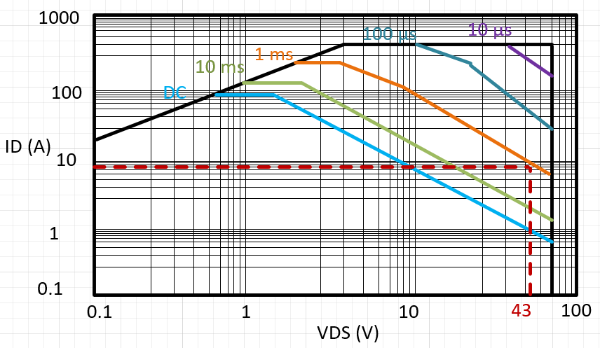
The current profile tapers down from 7 A to 0 A from the peak of 7 A as shown in Figure 9-5. The resulting average current (IISO_AVG) can be approximated as one third of the peak current that is around 2.4 A. The VDS clamp operation lasts for about 1 ms. Selecting a MOSFET with SOA characteristics covering the load line of 43 V which can support drain current greater than (IISO_PEAK/2) for 1 msec is a good starting point. For this particular design example, MOSFET which can support greater than 3.5 A of drain current at 43-V VDS on SoA curve is suitable.
Figure 9-2 shows typical SoA characteristics plot highlighting maximum drain current supported by the MOSFET for the duration of 1 ms. MOSFET data sheet SoA curves are typically plotted at ambient temperature, so consider sufficient margin over MOSFET parameters calculated values to ensure safe operation over desired operating temperature range.
 Figure 9-2 Typical MOSFET SoA Characteristics
As external MOSFET dissipates ISO7637-2 Pulse 1 energy, a special attention must be given while calculating maximum power dissipation and effective temperature rise. An average power dissipation across the MOSFET can be calculated by Equation 3.
For given design example, average power dissipation comes around.
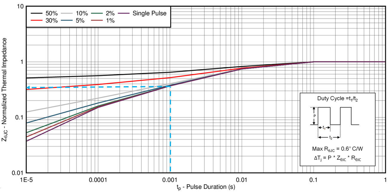
Typical ISO7637-2 pulse 1 transient lasts for 2 ms with total time period of 200 ms between two consecutive pulses (duty cycle of 1%). The effective temperature rise due to power dissipation across MOSFET during ISO7637-2 pulse 1 event can be calculated by looking at transient thermal impedance curve in a MOSFET data sheet. Figure 9-3 shows an example of how to estimate transient thermal impedance of a MOSFET for ISO7637-2 pulse 1 event.
 Figure 9-3 Typical MOSFET Transient Thermal Impedance
The maximum VGS LM74701-Q1 can drive is 13.9 V, so a MOSFET with 15-V minimum VGS rating must be selected.
Based on the design requirements and MOSFET selection criteria BUK7Y4R8-60E, SQJ460AEP, STL130N6F7 are some of the 60-V MOSFET options that can be selected.