JAJSMH7D April   2020  – May 2024 UCC27624

PRODUCTION DATA  

  1.   1
  2. 特長
  3. アプリケーション
  4. 概要
  5. Pin Configuration and Functions
  6. Specifications
    1. 5.1 Absolute Maximum Ratings
    2. 5.2 ESD Ratings
    3. 5.3 Recommended Operating Conditions
    4. 5.4 Thermal Information
    5. 5.5 Electrical Characteristics
    6. 5.6 Switching Characteristics
    7. 5.7 Timing Diagrams
    8. 5.8 Typical Characteristics
  7. Detailed Description
    1. 6.1 Overview
    2. 6.2 Functional Block Diagram
    3. 6.3 Feature Description
      1. 6.3.1 Operating Supply Current
      2. 6.3.2 Input Stage
      3. 6.3.3 Enable Function
      4. 6.3.4 Output Stage
      5. 6.3.5 Low Propagation Delays and Tightly Matched Outputs
    4. 6.4 Device Functional Modes
  8. Application and Implementation
    1. 7.1 Application Information
    2. 7.2 Typical Application
      1. 7.2.1 Design Requirements
      2. 7.2.2 Detailed Design Procedure
        1. 7.2.2.1 VDD and Undervoltage Lockout
        2. 7.2.2.2 Drive Current and Power Dissipation
      3. 7.2.3 Application Curves
  9. Power Supply Recommendations
  10. Layout
    1. 9.1 Layout Guidelines
    2. 9.2 Layout Example
    3. 9.3 Thermal Considerations
  11. 10Device and Documentation Support
    1. 10.1 Device Support
      1. 10.1.1 サード・パーティ製品に関する免責事項
    2. 10.2 ドキュメントの更新通知を受け取る方法
    3. 10.3 サポート・リソース
    4. 10.4 Trademarks
    5. 10.5 静電気放電に関する注意事項
    6. 10.6 用語集
  12. 11Revision History
  13. 12Mechanical, Packaging, and Orderable Information

Typical Characteristics

Unless otherwise specified, VDD=12 V, INx = 3.3 V, ENx = 3.3 V, TJ = 25°C, no load
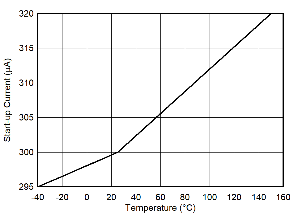
UCC27624 Start-Up and Quiescent
                        Current
Figure 5-3 Start-Up and Quiescent Current
UCC27624 Static Supply Current (Outputs in DC On or Off Condition)
Figure 5-5 Static Supply Current (Outputs in DC On or Off Condition)
UCC27624 VDD
                        UVLO Threshold
Figure 5-7 VDD UVLO Threshold
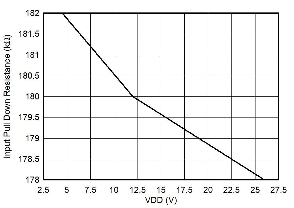
UCC27624 Input
                        Pulldown Resistance
Figure 5-9 Input Pulldown Resistance
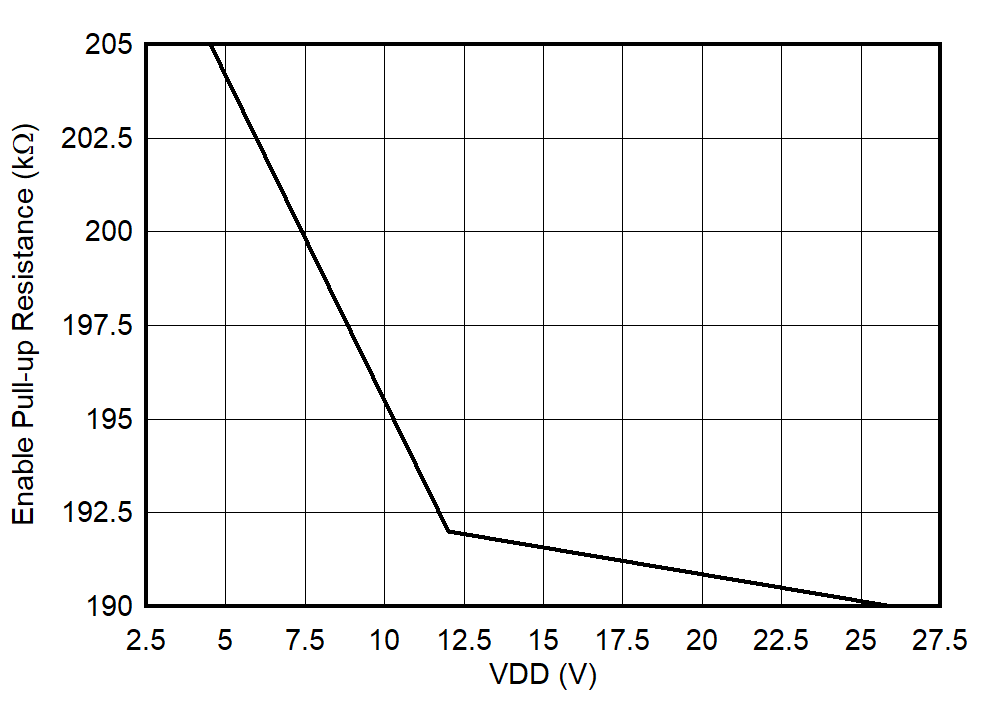
UCC27624 Enable Pullup Resistance
Figure 5-11 Enable Pullup Resistance
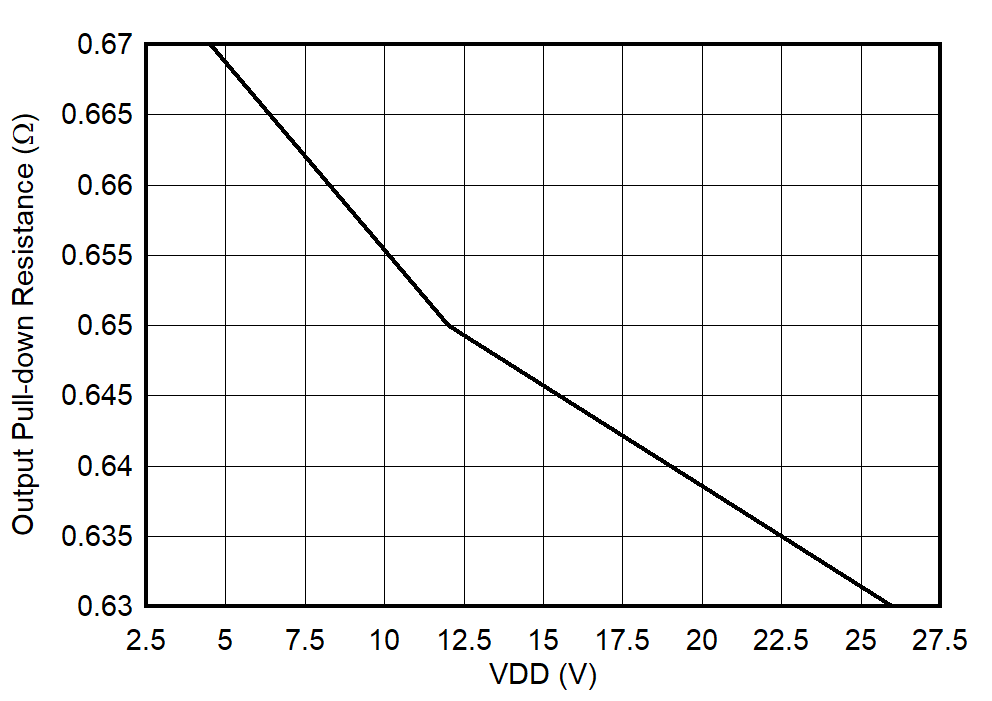
UCC27624 Output Pulldown Resistance
Figure 5-13 Output Pulldown Resistance
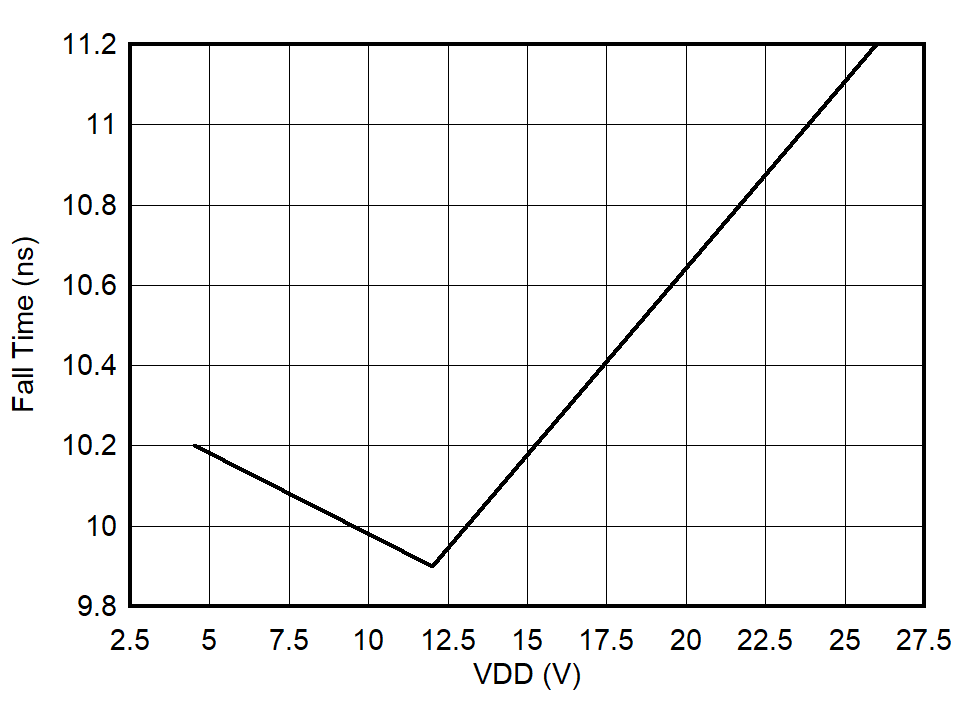
UCC27624 Output Fall Time vs VDD
CLOAD = 1.8 nF
Figure 5-15 Output Fall Time vs VDD
UCC27624 Input
                        to Output Rising (Turn-On) Propagation Delay vs VDD
CLOAD = 1.8 nF
Figure 5-17 Input to Output Rising (Turn-On) Propagation Delay vs VDD
UCC27624 Input Propagation Delay vs
                        Temperature
CLOAD = 1.8 nF
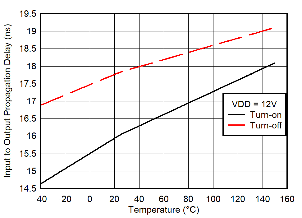
Figure 5-19 Input Propagation Delay vs Temperature
UCC27624 Enable to Output Falling Propagation Delay
CLOAD = 1.8 nF
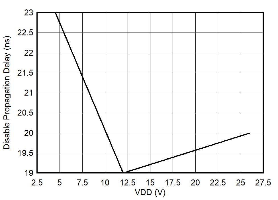
Figure 5-21 Enable to Output Falling Propagation Delay
UCC27624 Turn-Off and Falling Delay Matching
Figure 5-23 Turn-Off and Falling Delay Matching
UCC27624 Peak
                        Sink Current vs VDD
Figure 5-25 Peak Sink Current vs VDD
UCC27624 Operating Supply Current (Both Outputs Switching)
Figure 5-4 Operating Supply Current (Both Outputs Switching)
UCC27624 Disable Current (EN = 0 V)
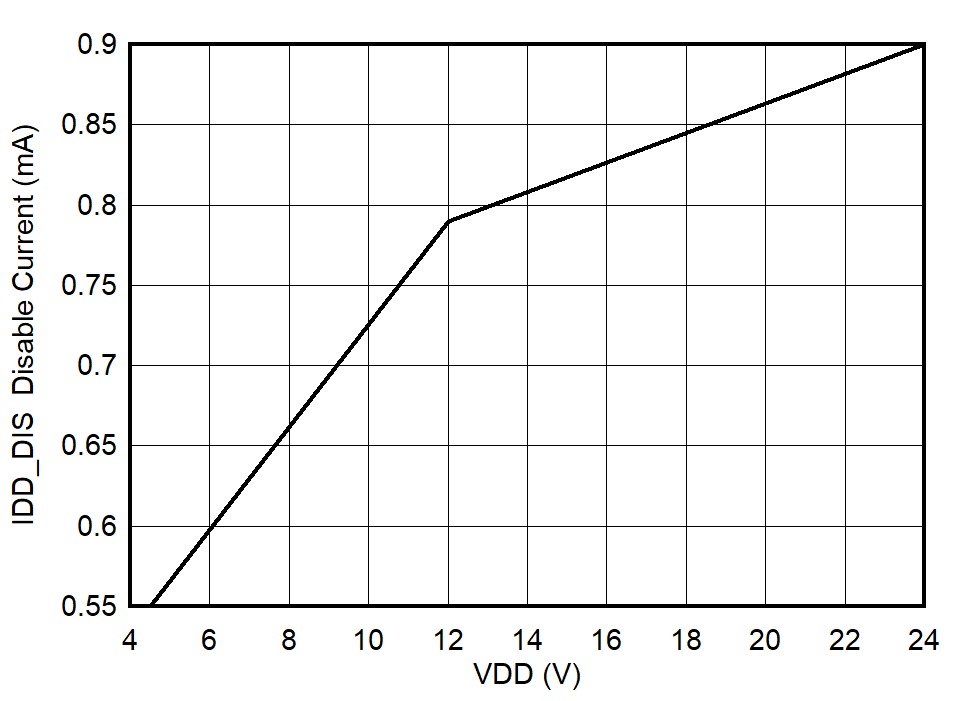
Figure 5-6 Disable Current (EN = 0 V)
UCC27624 Input
                        Thresholds
Figure 5-8 Input Thresholds
UCC27624 Enable Threshold
Figure 5-10 Enable Threshold
UCC27624 Output Pullup Resistance
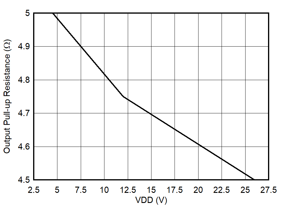
Figure 5-12 Output Pullup Resistance
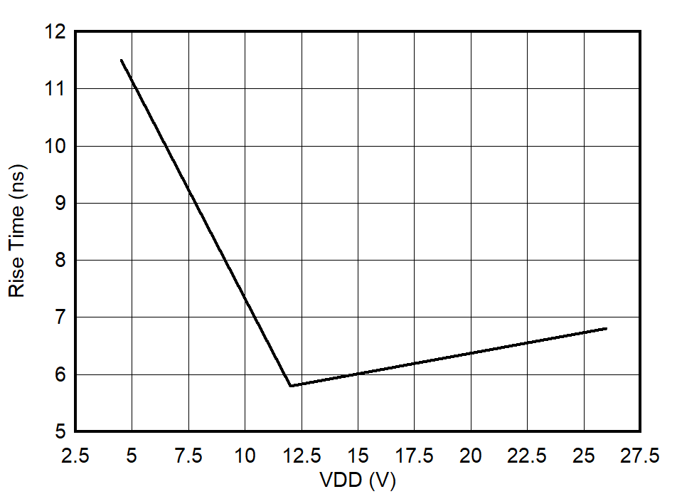
UCC27624 Output Rise Time vs VDD
CLOAD = 1.8 nF
Figure 5-14 Output Rise Time vs VDD
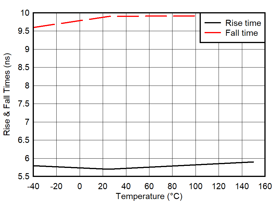
UCC27624 Output Rise
                        and
                        Fall Time vs Temperature
CLOAD = 1.8 nF
Figure 5-16 Output Rise and Fall Time vs Temperature
UCC27624 Input
                        to Output Falling (Turn-Off) Propagation Delay vs VDD
CLOAD = 1.8 nF
Figure 5-18 Input to Output Falling (Turn-Off) Propagation Delay vs VDD
UCC27624 Enable to Output Rising Propagation Delay
CLOAD = 1.8 nF
Figure 5-20 Enable to Output Rising Propagation Delay
UCC27624 Turn-on/Rising Delay Matching
Figure 5-22 Turn-on/Rising Delay Matching
UCC27624 Peak
                        Source Current vs VDD
Figure 5-24 Peak Source Current vs VDD