JAJSN20 September 2021 TPS25854-Q1 , TPS25855-Q1
PRODUCTION DATA
- 1 特長
- 2 アプリケーション
- 3 概要
- 4 Revision History
- 5 概要 (続き)
- 6 Device Comparison Table
- 7 Pin Configuration and Functions
- 8 Specifications
- 9 Parameter Measurement Information
-
10Detailed Description
- 10.1 Overview
- 10.2 Functional Block Diagram
- 10.3
Feature Description
- 10.3.1 Power Down or Undervoltage Lockout
- 10.3.2 Input Overvoltage Protection (OVP) - Continuously Monitored
- 10.3.3 Buck Converter
- 10.3.4 FREQ/SYNC
- 10.3.5 Bootstrap Voltage (BOOT)
- 10.3.6 Minimum ON-time, Minimum OFF-time
- 10.3.7 Internal Compensation
- 10.3.8 Current Limit and Short Circuit Protection
- 10.3.9 Cable Compensation
- 10.3.10 Thermal Management With Temperature Sensing (TS) and OTSD
- 10.3.11 Thermal Shutdown
- 10.3.12 FAULT Indication
- 10.3.13 USB Specification Overview
- 10.3.14 USB Type-C® Basics
- 10.3.15 USB Port Operating Modes
- 10.4 Device Functional Modes
-
11Application and Implementation
- 11.1 Application Information
- 11.2
Typical Applications
- 11.2.1 Design Requirements
- 11.2.2
Detailed Design Procedure
- 11.2.2.1 Output Voltage Setting
- 11.2.2.2 Switching Frequency
- 11.2.2.3 Inductor Selection
- 11.2.2.4 Output Capacitor Selection
- 11.2.2.5 Input Capacitor Selection
- 11.2.2.6 Bootstrap Capacitor Selection
- 11.2.2.7 Undervoltage Lockout Set-Point
- 11.2.2.8 Cable Compensation Set-Point
- 11.2.2.9 FAULT, POL, and THERM_WARN Resistor Selection
- 11.2.3 Application Curves
- 12Power Supply Recommendations
- 13Layout
- 14Device and Documentation Support
- 15Mechanical, Packaging, and Orderable Information
10.3.8.1 USB Switch Programmable Current Limit (ILIM)
Because the TPS2585x-Q1 integrates an USB current-limit switches, it provides adjustable current limit to prevent USB port overheating. The device engages the two-level current limit scheme, which has one typical current limit, IOS_BUS, and the secondary current limit, IOS_HI. The secondary current limit, IOS_HI, is 1.6 times the primary current limit, IOS_BUS. The secondary current limit acts as the current limit threshold for a deglitch time, tIOS_HI_DEG, then the USB power switch current limit threshold is set back to IOS_BUS. Equation 9 calculates the value of resistor for adjusting the typical current limit.

This equation assumes an ideal-no variation-external adjusting resistor. To take resistor tolerance into account, first determine the minimum and maximum resistor values based on its tolerance specifications and use these values in the equations. Because of the inverse relationship between the current limit and the adjusting resistor, use the maximum resistor value in the IOS(min) equation and the minimum resistor value in the IOS(max) equation. Table 10-2 lists the typical RILIM resistor value.
| RILIM (KΩ) | IOS_BUS - Current Limit Threshold (mA) |
|---|---|
| 19.1 | 1690 |
| 15.4 | 2096 |
| 11.5 | 2806 |
| 9.53 | 3386 |
| Short to GND | 3550 |
For the normal application, it can short the ILIM pin to GND directly, which sets a default 3.55-A current limit with a maximum ±15% variation on each USB port to follow the Type-C specification. The TPS2585x-Q1 provides built-in soft-start circuitry that controls the rising slew rate of the output voltage to limit inrush current and voltage surges.
The secondary current limit, IOS_HI, allows the USB port pull out a larger current for a short time during transient overload conditions, which can bring benefits for USB port special overload testing like MFi OCP. In a normal application, once the device is powered on and USB port is not in UVLO, the USB port current limit threshold is overridden by the secondary current limit, IOS_HI, so the USB port can output as high as a 1.6 × IOS_BUS current for typically 2 ms. After the deglitch time, tIOS_HI_DEG, the current limit threshold is set back to the typical current with IOS_BUS. The secondary current limit threshold does not resume until after the tIOS_HI_RST deglitch time, which is typically 16 ms. If there is an inrush current higher than the IOS_HI threshold, the current limit is set back to IOS_BUS immediately, without waiting for a tIOS_HI_DEG.
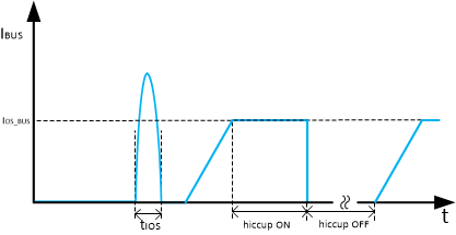
The TPS2585x-Q1 responds to overcurrent conditions by limiting output current to IOS_BUS as shown in previous equation. When an overload condition occurs, the device maintains a constant output current and the output voltage reduces accordingly. Three possible overload conditions can occur:
- The first condition is when a short circuit or overload is
applied to the USB output when the device is powered up or enabled. There can be
inrush current and once it triggers the approximate 8-A threshold, a fast
turnoff circuit is activated to turn off the USB power switch within
tIOS_USB before the current limit control loop is able to respond
(shown in Figure 10-5). After the fast turnoff is triggered, the USB power switch current-sense
amplifier is over-driven during this time and momentarily disables the internal
N-channel MOSFET to turn off USB port. The current-sense amplifier then recovers
and ramps the output current with a soft start. If the USB port is still in
overcurrent condition, the short circuit and overload hold the output near zero
potential with respect to ground and the power switch ramps the output current
to IOS_BUS. If the overcurrent limit condition lasts longer than 4.1
ms, the corresponding USB channel enters hiccup mode with 524 ms of off-time and
4.1 ms of on-time.
 Figure 10-5 Response Time to BUS
Short-Circuit
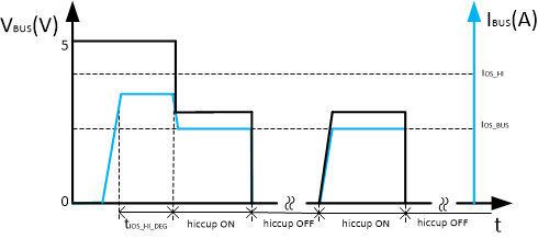
 - The second condition is the load current increases above
IOS_BUS but below the IOS_HI setting. The device
allows the USB port to output this large current for tIOS_HI_DEG,
without limiting the USB port current to IOS_BUS. After the
tIOS_HI_DEG deglitch time, the device limits the output current
to IOS_BUS and works in a constant current-limit mode. If the load
demands a current greater than IOS_BUS, the USB output voltage
decreases to IOS_BUS × RLOAD for a resistive load, which
is shown in Figure 10-6. If the overcurrent limit condition lasts longer than 4.1 ms, the
corresponding USB channel enters hiccup mode with 524 ms of off-time and 4.1 ms
of on-time. Another USB channel still works normally.
 Figure 10-6 BUS Overcurrent
Protection
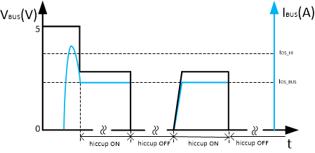
 - The third condition is the load current increases just over the IOS_HI setting. In this case, the load current does not trigger the fast turnoff. The USB power switch current limit threshold is set back to the primary current limit, IOS_BUS, immediately. If the load still demands a current greater than IOS_BUS, the USB output voltage decreases to IOS_BUS × RLOAD for a resistive load, which is shown in Figure 10-7. If the overcurrent limit condition lasts longer than 4.1 ms, the corresponding USB channel enters hiccup mode with 524 ms of off-time and 4.1 ms of on-time. Another USB channel still works normally.
 Figure 10-7 BUS Overcurrent Protection:
Two-Level Current Limit
Figure 10-7 BUS Overcurrent Protection:
Two-Level Current LimitThe TPS2585x-Q1 thermal cycles if an overload condition is present long enough to activate thermal limiting in any of the previously mentioned cases. Thermal limiting turns off the internal NFET and starts when the NFET junction temperature exceeds 160°C (typical). The device remains off until the NFET junction temperature cools 10°C (typical) and then restarts. This extra thermal protection mechanism can help prevent further junction temperature rise, which can cause the device to turn off due to junction temperature exceeding the main thermal shutdown threshold, TSD.