JAJSN20 September 2021 TPS25854-Q1 , TPS25855-Q1
PRODUCTION DATA
- 1 特長
- 2 アプリケーション
- 3 概要
- 4 Revision History
- 5 概要 (続き)
- 6 Device Comparison Table
- 7 Pin Configuration and Functions
- 8 Specifications
- 9 Parameter Measurement Information
-
10Detailed Description
- 10.1 Overview
- 10.2 Functional Block Diagram
- 10.3
Feature Description
- 10.3.1 Power Down or Undervoltage Lockout
- 10.3.2 Input Overvoltage Protection (OVP) - Continuously Monitored
- 10.3.3 Buck Converter
- 10.3.4 FREQ/SYNC
- 10.3.5 Bootstrap Voltage (BOOT)
- 10.3.6 Minimum ON-time, Minimum OFF-time
- 10.3.7 Internal Compensation
- 10.3.8 Current Limit and Short Circuit Protection
- 10.3.9 Cable Compensation
- 10.3.10 Thermal Management With Temperature Sensing (TS) and OTSD
- 10.3.11 Thermal Shutdown
- 10.3.12 FAULT Indication
- 10.3.13 USB Specification Overview
- 10.3.14 USB Type-C® Basics
- 10.3.15 USB Port Operating Modes
- 10.4 Device Functional Modes
-
11Application and Implementation
- 11.1 Application Information
- 11.2
Typical Applications
- 11.2.1 Design Requirements
- 11.2.2
Detailed Design Procedure
- 11.2.2.1 Output Voltage Setting
- 11.2.2.2 Switching Frequency
- 11.2.2.3 Inductor Selection
- 11.2.2.4 Output Capacitor Selection
- 11.2.2.5 Input Capacitor Selection
- 11.2.2.6 Bootstrap Capacitor Selection
- 11.2.2.7 Undervoltage Lockout Set-Point
- 11.2.2.8 Cable Compensation Set-Point
- 11.2.2.9 FAULT, POL, and THERM_WARN Resistor Selection
- 11.2.3 Application Curves
- 12Power Supply Recommendations
- 13Layout
- 14Device and Documentation Support
- 15Mechanical, Packaging, and Orderable Information
10.3.14.1 Configuration Channel
The function of the configuration channel is to detect connections and configure the interface across the USB Type-C cables and connectors.
Functionally the Configuration Channel (CC) is used to serve the following purposes:
- Detect connect to the USB ports
- Resolve cable orientation and twist connections to establish USB data bus routing
- Establish DFP and UFP roles between two connected ports
- Discover and configure power: USB Type-C current modes or USB Power Delivery
- Discovery and configure optional Alternate and Accessory modes
- Enhance flexibility and ease of use
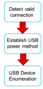
Typical flow of DFP to UFP configuration is shown in Figure 10-13:
 Figure 10-13 Flow of DFP to UFP Configuration