JAJSNA6O December 2012 – August 2024 TPD1E05U06 , TPD4E05U06 , TPD6E05U06
PRODUCTION DATA
- 1
- 1 特長
- 2 アプリケーション
- 3 概要
- 4 Pin Configuration and Functions
- 5 Specifications
- 6 Detailed Description
- 7 Application and Implementation
- 8 Device and Documentation Support
- 9 Revision History
- 10Mechanical, Packaging, and Orderable Information
4 Pin Configuration and Functions
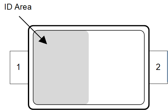
 Figure 4-1 DPY Package 2-Pin X1SON
(Top View)
 Figure 4-2 DYA Package 2-Pin SOD-523
(Top View)
Figure 4-2 DYA Package 2-Pin SOD-523
(Top View)Table 4-1 Pin Functions TPD1E05U06 DPY
and DYA
| PIN | TYPE(1) | DESCRIPTION | |
|---|---|---|---|
| NAME | NO. | ||
| GND | 2 | Ground | Ground; Connect to ground |
| I/O | 1 | I/O | ESD protected channel(2) |
(1) I = input, O = output
(2) Place as close to the connector as possible.
 Figure 4-3 DQA Package 10-Pin USON (Top
View)
Figure 4-3 DQA Package 10-Pin USON (Top
View)Table 4-2 Pin Functions TPD4E05U06
DQA
| PIN | TYPE(1) | DESCRIPTION | |
|---|---|---|---|
| NAME | NO. | ||
| D1+ | 1 | I/O | ESD protected channel(2) |
| D1– | 2 | I/O | ESD protected channel(2) |
| D2+ | 4 | I/O | ESD protected channel(2) |
| D2– | 5 | I/O | ESD protected channel(2) |
| GND | 3 | Ground | Ground; Connect to ground |
| GND | 8 | ||
| NC | 6 | — | Not connected; Used for optional straight-through routing. Can be left floating or grounded |
| NC | 7 | ||
| NC | 9 | ||
| NC | 10 | ||
(1) I = input, O = output
(2) Place as close to the connector as possible.
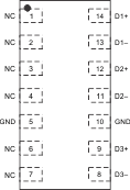
 Figure 4-4 RVZ Package 14-Pin USON (Top
View)
Figure 4-4 RVZ Package 14-Pin USON (Top
View)Table 4-3 Pin Functions TPD6E05U06
RVZ
| PIN | TYPE(1) | DESCRIPTION | |
|---|---|---|---|
| NAME | NO. | ||
| D1+ | 14 | I/O | ESD protected channel(2) |
| D1– | 13 | I/O | ESD protected channel(2) |
| D2+ | 12 | I/O | ESD protected channel(2) |
| D2– | 11 | I/O | ESD protected channel(2) |
| D3+ | 9 | I/O | ESD protected channel(2) |
| D3– | 8 | I/O | ESD protected channel(2) |
| GND | 5 | Ground | Ground; Connect to ground |
| GND | 10 | ||
| NC | 1 | — | Not connected; Used for optional straight-through routing. Can be left floating or grounded |
| NC | 2 | ||
| NC | 3 | ||
| NC | 4 | ||
| NC | 6 | ||
| NC | 7 | ||
(1) I = input, O = output
(2) Place as close to the connector as possible.