JAJSNI4 December 2021 DAC11001B
PRODUCTION DATA
- 1 特長
- 2 アプリケーション
- 3 概要
- 4 Revision History
- 5 Pin Configuration and Functions
-
6 Specifications
- 6.1 Absolute Maximum Ratings
- 6.2 ESD Ratings
- 6.3 Recommended Operating Conditions
- 6.4 Thermal Information
- 6.5 Electrical Characteristics
- 6.6 Timing Requirements: Write, 4.5 V ≤ DVDD ≤ 5.5 V
- 6.7 Timing Requirements: Write, 2.7 V ≤ DVDD < 4.5 V
- 6.8 Timing Requirements: Read and Daisy-Chain Write, 4.5 V ≤ DVDD ≤ 5.5 V
- 6.9 Timing Requirements: Read and Daisy-Chain Write, 2.7 V ≤ DVDD < 4.5 V
- 6.10 Timing Diagrams
- 6.11 Typical Characteristics
-
7 Detailed Description
- 7.1 Overview
- 7.2 Functional Block Diagram
- 7.3 Feature Description
- 7.4 Device Functional Modes
- 7.5 Programming
- 7.6
Register Map
- 7.6.1 NOP Register (address = 00h) [reset = 0x000000h for bits [23:0]]
- 7.6.2 DAC-DATA Register (address = 01h) [reset = 0x000000h for bits [23:0]]
- 7.6.3 CONFIG1 Register (address = 02h) [reset = 004C80h for bits [23:0]]
- 7.6.4 DAC-CLEAR-DATA Register (address = 03h) [reset = 000000h for bits [23:0]]
- 7.6.5 TRIGGER Register (address = 04h) [reset = 000000h for bits [23:0]]
- 7.6.6 STATUS Register (address = 05h) [reset = 000000h for bits [23:0]]
- 7.6.7 CONFIG2 Register (address = 06h) [reset = 000040h for bits [23:0]]
- 8 Application and Implementation
- 9 Power Supply Recommendations
- 10Layout
- 11Device and Documentation Support
- 12Mechanical, Packaging, and Orderable Information
9 Power Supply Recommendations
To get the best performance out of the DAC11001B, the power supply, grounding, and decoupling are very important. Use a PCB with a ground-plane reference, which helps in confining the digital return currents. A low mutual inductance path is created just beneath the high-frequency digital traces causing the return currents to follow the respective signal traces, thus minimizing crosstalk. On the other hand, dc signals spread over the ground plane without being confined below the signal trace. Therefore, in precision dc applications, limiting the common-impedance coupling is very difficult unless the ground planes are physically separated. Figure 9-1 shows a method to divide the grounds so that there is no common-mode current flow between the grounds, while maintaining the same dc potential across all grounds. This circuit assumes that the REFGND and LOAD-GND are provided from isolated power sources, therefore, there is no common-mode current flow through the reference or the load.
When the load circuit is powered from a source referenced to AGND, and the LOAD-GND is shorted to AGND at the far end, the AGND-OUT must no longer be shorted to AGND locally near the DAC. The local shorting creates a ground loop, otherwise. The resulting connection that avoids the ground loop is shown in Figure 9-2.
When the reference source is powered from a power source with AGND as the ground, there is a possibility of common-impedance coupling causing a code-dependent shift in the reference voltage. To avoid undesired coupling, drive REFGND using a buffer that maintains the reference ground potential equals to that of AGND-OUT, as shown in Figure 9-3.
Channel-to-channel dc crosstalk is a major concern in multichannel applications, such as battery test equipment. While the DAC11001B is single-channel, the crosstalk problem can appear at a system level when using multiple DAC11001B devices. The problem becomes severe when the grounds of the loads are shorted together creating a possible ground loop. In such cases, avoid the local short between AGND and AGND-OUT. Use a single short between AGND and DGND for all the DACs. If the PCB layout allows for the digital signal and analog power supplies to be kept separate, DGND and AGND can be combined to a single ground plane. Figure 9-4 shows an example circuit for minimizing dc crosstalk across DAC channels in a system.
Power-supply bypassing and decoupling is key to keeping power supply noise, switching transients, and common-mode currents away from the DAC output. There are three main objective of power-supply bypassing:
- Filtering: Filter out noise and ripple from power supplies
- Bypassing: Supply switching or load transient currents locally by avoiding trace inductances
- Decoupling: Stop local transient currents from impacting other circuits
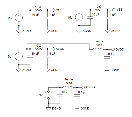
To achieve these objectives, use the following 3-element scheme. Place a decoupling capacitor close to every power supply pin to provide the local current path for load and circuit switching transients. This capacitor must be referenced to the respective load ground for best load transient suppression. Use a 0.1-µF to 1-µF, X7R, multilayer ceramic capacitor (MLCC) for this purpose. For analog power supplies, a 10-Ω series resistor provides the best decoupling. For filtering the power-supply noise and ripple, 10-µF capacitors work best when placed at the power entry point of the board. An example decoupling scheme is shown in Figure 9-5.
 Figure 9-5 Power-Supply
Decoupling