JAJSNW1B October 2023 – June 2024 TPSM843620
PRODUCTION DATA
- 1
- 1 特長
- 2 アプリケーション
- 3 概要
- 4 Pin Configuration and Functions
- 5 Specifications
-
6 Detailed Description
- 6.1 Overview
- 6.2 Functional Block Diagram
- 6.3
Feature Description
- 6.3.1 VIN Pins and VIN UVLO
- 6.3.2 Enable and Adjustable UVLO
- 6.3.3 Adjusting the Output Voltage
- 6.3.4 Switching Frequency Selection
- 6.3.5 Switching Frequency Synchronization to an External Clock
- 6.3.6 Ramp Amplitude Selection
- 6.3.7 Soft Start and Prebiased Output Start-Up
- 6.3.8 Mode Pin
- 6.3.9 Power Good (PGOOD)
- 6.3.10 Current Protection
- 6.3.11 Output Overvoltage and Undervoltage Protection
- 6.3.12 Overtemperature Protection
- 6.3.13 Output Voltage Discharge
- 6.4 Device Functional Modes
-
7 Application and Implementation
- 7.1 Application Information
- 7.2
Typical Applications
- 7.2.1
1.0V Output, 1MHz
Application
- 7.2.1.1 Design Requirements
- 7.2.1.2
Detailed Design Procedure
- 7.2.1.2.1 Switching Frequency
- 7.2.1.2.2 Output Inductor Selection
- 7.2.1.2.3 Output Capacitor
- 7.2.1.2.4 Input Capacitor
- 7.2.1.2.5 Adjustable Undervoltage Lockout
- 7.2.1.2.6 Output Voltage Resistors Selection
- 7.2.1.2.7 Bootstrap Capacitor Selection
- 7.2.1.2.8 BP5 Capacitor Selection
- 7.2.1.2.9 PGOOD Pullup Resistor
- 7.2.1.2.10 Current Limit Selection
- 7.2.1.2.11 Soft-Start Time Selection
- 7.2.1.2.12 Ramp Selection and Control Loop Stability
- 7.2.1.2.13 MODE Pin
- 7.2.1.3 Application Curves
- 7.2.1
1.0V Output, 1MHz
Application
- 7.3 Power Supply Recommendations
- 7.4 Layout
- 8 Device and Documentation Support
- 9 Revision History
- 10Mechanical, Packaging, and Orderable Information
6.3.5.3 Interfacing the SYNC/FSEL Pin
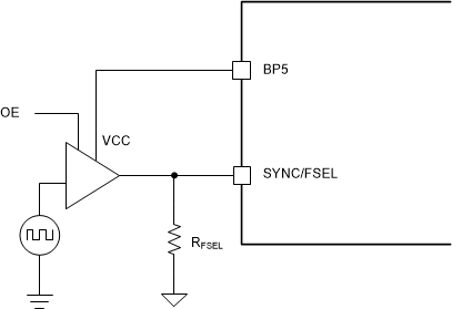
If an application requires synchronizing to a SYNC clock but the clock is unavailable before the device is enabled, TI recommends a high impedance buffer to make sure of proper detection of the RFSEL value. Figure 6-5 shows the recommended implementation. The leakage current into the buffer output must be less than 5µA to make sure of proper detection of the RFSEL value. Power the buffer from the BP5 output of the device to make sure the VCC voltage is available and the buffers output is high impedance before the device tries to detect the RFSEL value. When powering the buffer from the BP5 pin, the external load on the BP5 pin must be less than 2 mA.
 Figure 6-5 Interfacing the SYNC/FSEL Pin With a
Buffer