JAJSOR1E June 2022 – August 2024 LM5177
PRODUCTION DATA
- 1
- 1 特長
- 2 アプリケーション
- 3 概要
- 4 Pin Configuration and Functions
- 5 Specifications
- 6 Parameter Measurement Information
-
7 Detailed Description
- 7.1 Overview
- 7.2 Functional Block Diagram
- 7.3
Feature Description
- 7.3.1 Power-On Reset (POR System)
- 7.3.2 Buck-Boost Control Scheme
- 7.3.3 Power Save Mode
- 7.3.4 Supply Voltage Selection – VMAX Switch
- 7.3.5 Enable and Undervoltage Lockout
- 7.3.6 Oscillator Frequency Selection
- 7.3.7 Frequency Synchronization
- 7.3.8 Voltage Regulation Loop
- 7.3.9 Output Voltage Tracking
- 7.3.10 Slope Compensation
- 7.3.11 Configurable Soft Start
- 7.3.12 Peak Current Sensor
- 7.3.13 Current Monitoring and Current Limit Control Loop
- 7.3.14 Short Circuit - Hiccup Protection
- 7.3.15 nFLT Pin and Protections
- 7.3.16 Device Configuration Pin
- 7.3.17 Dual Random Spread Spectrum – DRSS
- 7.3.18 Gate Driver
- 7.4 Device Functional Modes
-
8 Application and Implementation
- 8.1 Application Information
- 8.2
Typical Application
- 8.2.1 Design Requirements
- 8.2.2
Detailed Design Procedure
- 8.2.2.1 Custom Design with WEBENCH Tools
- 8.2.2.2 Frequency
- 8.2.2.3 Feedback Divider
- 8.2.2.4 Inductor and Current Sense Resistor Selection
- 8.2.2.5 Slope Compensation
- 8.2.2.6 Output Capacitor
- 8.2.2.7 Input Capacitor
- 8.2.2.8 UVLO Divider
- 8.2.2.9 Soft-Start Capacitor
- 8.2.2.10 MOSFETs QH1 and QL1
- 8.2.2.11 MOSFETs QH2 and QL2
- 8.2.2.12 Frequency Compensation
- 8.2.2.13 External Component Selection
- 8.2.3 Application Curves
- 8.3 System Examples
- 9 Power Supply Recommendations
- 10Layout
- 11Device and Documentation Support
- 12Revision History
- 13Mechanical, Packaging, and Orderable Information
7.3.13 Current Monitoring and Current Limit Control Loop
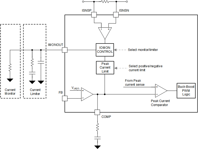
The LM5177 features two high voltage current sensors. The first one maintains the peak current sensing between the CSA and CSB pins. The second current sensor inputs are connected to the ISNSP and ISNSN pins.
This optional current sensing provides the capability to monitor or to limit either the input or the output current of the DC/DC converter If the optional current sense amplifier is not used, the user can disable it to reduce the bias current consumption of the whole device by connecting the IMONOUT pin to VCC. Do not do this dynamical during the operation of the device because the configuration gets latched at start-up of the converter. Use the CFG pin to select one of the following desired operation modes.
Current Monitor Operation:
In case the current sense amplifier is configured as a monitor, the output voltage on the IMONOUT pin is a linear relation between the sense voltage between ISNSP and ISNSN pins and the sense amplifier transcendence as well as the resistor placed on the IMONOUT pin:
The output voltage of the IMONOUT pin is clamped to the values given in specifications section.
If the user intends to reduce the bandwidth of the current monitor, the user can place an optional capacitor in parallel to the IMONOUT pin like it is indicated in Figure 7-17.
Current Limit Operation:
In this configuration, the current sense gm amplifier monitors the voltage across the sense resistor and compares it with an internal reference voltage. If the drop across the sense resistor is greater than the reference threshold the gm amplifier gradually reduces the peak current capability of the DC/DC converter until the differential voltage is equal the reference voltage. This function of the LM5177 can be used to do the following:
- Regulate the current into the load from the power stage
- Regulate the current from the output into the power stage
- Regulated the current from the input supply to the power stage
- Regulated the current into the device input from the power stage
Once the current limit operation mode is selected, a RC compensation network must be placed on the IMONOUT pin. For most applications, a compensation bandwidth with a factor of 3× to 5× faster than the compensation of the output voltage loop has given good results.
 Figure 7-17 Current Monitor Functional
Block Diagram