JAJSOR1E June 2022 – August 2024 LM5177
PRODUCTION DATA
- 1
- 1 特長
- 2 アプリケーション
- 3 概要
- 4 Pin Configuration and Functions
- 5 Specifications
- 6 Parameter Measurement Information
-
7 Detailed Description
- 7.1 Overview
- 7.2 Functional Block Diagram
- 7.3
Feature Description
- 7.3.1 Power-On Reset (POR System)
- 7.3.2 Buck-Boost Control Scheme
- 7.3.3 Power Save Mode
- 7.3.4 Supply Voltage Selection – VMAX Switch
- 7.3.5 Enable and Undervoltage Lockout
- 7.3.6 Oscillator Frequency Selection
- 7.3.7 Frequency Synchronization
- 7.3.8 Voltage Regulation Loop
- 7.3.9 Output Voltage Tracking
- 7.3.10 Slope Compensation
- 7.3.11 Configurable Soft Start
- 7.3.12 Peak Current Sensor
- 7.3.13 Current Monitoring and Current Limit Control Loop
- 7.3.14 Short Circuit - Hiccup Protection
- 7.3.15 nFLT Pin and Protections
- 7.3.16 Device Configuration Pin
- 7.3.17 Dual Random Spread Spectrum – DRSS
- 7.3.18 Gate Driver
- 7.4 Device Functional Modes
-
8 Application and Implementation
- 8.1 Application Information
- 8.2
Typical Application
- 8.2.1 Design Requirements
- 8.2.2
Detailed Design Procedure
- 8.2.2.1 Custom Design with WEBENCH Tools
- 8.2.2.2 Frequency
- 8.2.2.3 Feedback Divider
- 8.2.2.4 Inductor and Current Sense Resistor Selection
- 8.2.2.5 Slope Compensation
- 8.2.2.6 Output Capacitor
- 8.2.2.7 Input Capacitor
- 8.2.2.8 UVLO Divider
- 8.2.2.9 Soft-Start Capacitor
- 8.2.2.10 MOSFETs QH1 and QL1
- 8.2.2.11 MOSFETs QH2 and QL2
- 8.2.2.12 Frequency Compensation
- 8.2.2.13 External Component Selection
- 8.2.3 Application Curves
- 8.3 System Examples
- 9 Power Supply Recommendations
- 10Layout
- 11Device and Documentation Support
- 12Revision History
- 13Mechanical, Packaging, and Orderable Information
7.3.17 Dual Random Spread Spectrum – DRSS
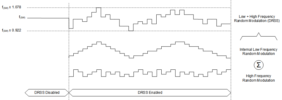
The device provides a digital spread spectrum, which reduces the EMI of the power supply over a wide frequency range. This function is enabled by the CFG pin. When the spread spectrum is enabled, the internal modulator dithers the internal clock. When an external synchronization clock is applied to the SYNC pin, the internal spread spectrum is disabled. DRSS combines a low frequency triangular modulation profile with a high frequency cycle-by-cycle random modulation profile. The low frequency triangular modulation improves performance in lower radio frequency bands (for example, AM band), while the high frequency random modulation improves performance in higher radio frequency bands (for example, FM band). In addition, the frequency of the triangular modulation is further modulated randomly to reduce the likelihood of any audible tones. To minimize output voltage ripple caused by spread spectrum, duty cycle is modified on a cycle-by-cycle basis to maintain a nearly constant duty cycle when dithering is enabled.

Figure 7-19 Dual Random Spread Spectrum