JAJSOU4C November   2011  – June 2022 TPA2015D1

PRODUCTION DATA  

  1. 特長
  2. アプリケーション
  3. 説明
  4. Revision History
  5. Device Comparison Table
  6. Pin Configuration and Functions
  7. Specifications
    1. 7.1 Absolute Maximum Ratings
    2. 7.2 ESD Ratings
    3. 7.3 Recommended Operating Conditions
    4. 7.4 Thermal Information
    5. 7.5 Electrical Characteristics
    6. 7.6 Operating Characteristics
    7. 7.7 Typical Characteristics
  8. Parameter Measurement Information
  9. Detailed Description
    1. 9.1 Overview
    2. 9.2 Functional Block Diagram
    3. 9.3 Feature Description
      1. 9.3.1 SpeakerGuard™ Theory of Operation
        1. 9.3.1.1 SpeakerGuard™ With Varying Input Levels
        2. 9.3.1.2 Battery Tracking SpeakerGuard™
      2. 9.3.2 Fully Differential Class-D Amplifier
        1. 9.3.2.1 Advantages of Fully Differential Amplifiers
        2. 9.3.2.2 Improved Class-D Efficiency
      3. 9.3.3 Adaptive Boost Converter
        1. 9.3.3.1 Boost Converter Overvoltage Protection
      4. 9.3.4 Operation With DACs and CODECs
      5. 9.3.5 Filter Free Operation and Ferrite Bead Filters
      6. 9.3.6 Speaker Load Limitation
      7. 9.3.7 Fixed Gain Setting
    4. 9.4 Device Functional Modes
      1. 9.4.1 Shutdown Mode
      2. 9.4.2 Battery Tracking SpeakerGuard™ Operation
  10. 10Application and Implementation
    1. 10.1 Application Information
    2. 10.2 Typical Applications
      1. 10.2.1 TPA2015D1 With Differential Input Signals
        1. 10.2.1.1 Design Requirements
        2. 10.2.1.2 Detailed Design Procedure
          1. 10.2.1.2.1 Boost Converter Inductor Selection
            1. 10.2.1.2.1.1 Inductor Equations
          2. 10.2.1.2.2 Boost Converter Capacitor Selection
          3. 10.2.1.2.3 Components Location and Selection
            1. 10.2.1.2.3.1 Decoupling Capacitors
            2. 10.2.1.2.3.2 Input Capacitors
        3. 10.2.1.3 Application Curves
      2. 10.2.2 TPA2015D1 with Single-Ended Input Signals
        1. 10.2.2.1 Design Requirements
        2. 10.2.2.2 Detailed Design Procedure
        3. 10.2.2.3 Application Curves
  11. 11Power Supply Recommendations
    1. 11.1 Power Supply Decoupling Capacitors
  12. 12Layout
    1. 12.1 Layout Guidelines
      1. 12.1.1 Component Placement
      2. 12.1.2 Trace Width
      3. 12.1.3 Pad Size
    2. 12.2 Layout Example
  13. 13Device and Documentation Support
    1. 13.1 Device Support
      1. 13.1.1 Device Nomenclature
        1. 13.1.1.1 TPA2015D1 Glossary
        2. 13.1.1.2 Boost Terms
    2. 13.2 Community Resources
    3. 13.3 Trademarks
  14. 14Mechanical, Packaging, and Orderable Information
    1. 14.1 Package Option Addendum
      1. 14.1.1 Packaging Information
      2. 14.1.2 Tape and Reel Information

Typical Characteristics

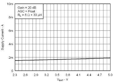
VBAT = 3.6 V, Gain = 6 dB, CI = 1 µF, CBOOST = 22 µF, LBOOST = 2.2 µH, AGC = Float, ENB = END = VBAT, and Load = 8 Ω + 33 µH unless otherwise specified.
GUID-52EC582F-F5F9-4121-9417-19BF60598B05-low.gif
Figure 7-1 Quiescent Supply Current vs Supply Voltage
GUID-C7A28CC4-0BD1-43FE-A25E-5CD33FAB3878-low.gif
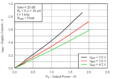
Figure 7-3 Supply Current vs Output Power
GUID-F30E350B-8496-4D52-9BB5-D9AE38770D39-low.gif
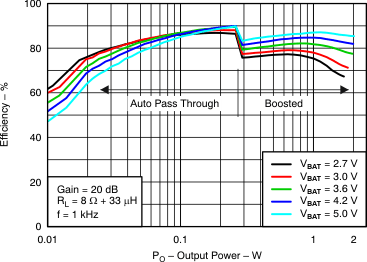
Figure 7-5 Total Efficiency vs Output Power
GUID-38AF8BCB-75BD-48B2-874F-31E869027BC9-low.gif
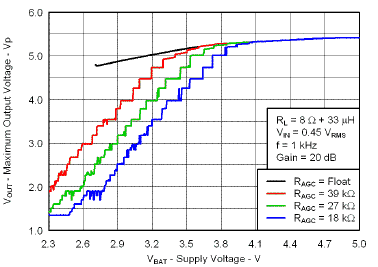
Figure 7-7 Maximum Output Voltage vs Supply Voltage
GUID-027D10EA-1AB1-4115-9461-8E8A43CBC075-low.gif
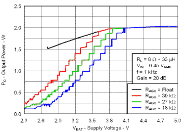
Figure 7-9 Output Power vs Supply Voltage
GUID-D63E9218-35CD-41E0-A9D0-F457D46DF833-low.gif
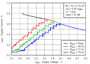
Figure 7-11 Supply Current vs Supply Voltage
GUID-D507CD34-C423-4B5A-966B-91A1835AAC60-low.gif
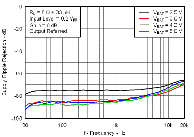
Figure 7-13 Supply Ripple Rejection vs Frequency
GUID-CB8189D8-40E3-4B43-860B-6A18A0770449-low.gif
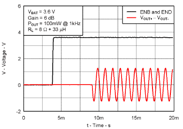
Figure 7-15 Startup Timing
GUID-CF3F8214-2AF5-4B68-BC7F-B8D733CC2266-low.png
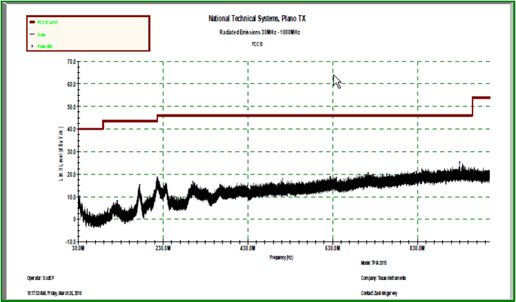
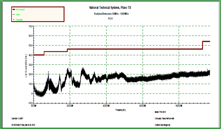
Figure 7-17 Emc Performance PO = 50 mW With 2 Inch Speaker Cable
GUID-1A38B70B-1062-43CE-A7AB-2064D9A57D7C-low.gif
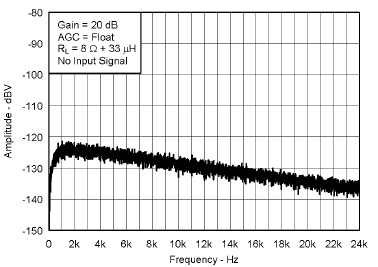
Figure 7-2 A-Weighted Output Noise vs Frequency
GUID-1A0DD5DD-ECCD-49C1-8F3D-C1415392ECF1-low.gif
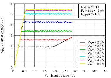
Figure 7-4 Peak Output Voltage vs Peak Input Voltage
GUID-EFD895D3-4BFF-4BA1-A4BC-21205B4D2765-low.gif
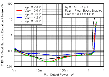
Figure 7-6 Total Harmonic Distortion + Noise vs Output Power
GUID-0C174BA1-372F-4108-B4FC-E48946D476E2-low.gif
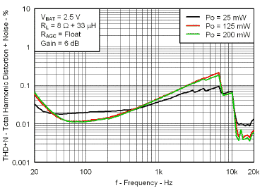
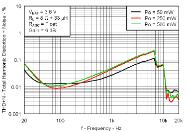
Figure 7-8 Total Harmonic Distortion + Noise vs Frequency
GUID-254E9C7A-5995-4FC0-B23D-D47108BE9B0B-low.gif
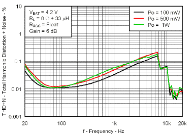
Figure 7-10 Total Harmonic Distortion + Noise vs Frequency
GUID-5778E05B-5671-44DA-B47F-AF451EC001AF-low.gif
Figure 7-12 Total Harmonic Distortion + Noise vs Frequency
GUID-1FB3B8FE-9626-4097-93F5-90A9F8068DD3-low.gif
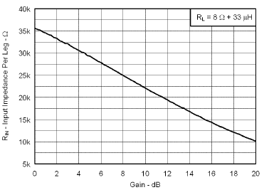
Figure 7-14 Input Impedance (Per Input) vs Gain
GUID-55FD6C14-042C-46CD-A07E-FE097BAE3625-low.gif
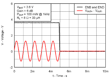
Figure 7-16 Shutdown Timing
GUID-4CCC53C1-0E87-4F2A-B652-B720BA938544-low.png
Figure 7-18 Emc Performance PO = 750 mW With 2 Inch Speaker Cable