JAJSPW8E march 2011 – february 2023 ADS4222 , ADS4225 , ADS4226 , ADS4242 , ADS4245 , ADS4246
PRODUCTION DATA
- 1 特長
- 2 アプリケーション
- 3 概要
- 4 Revision History
- 5 概要 (続き)
- 6 Pin Configuration and Functions
-
7 Specifications
- 7.1 Absolute Maximum Ratings
- 7.2 ESD Ratings
- 7.3 Recommended Operating Conditions
- 7.4 Thermal Information
- 7.5 Electrical Characteristics: ADS4246, ADS4245, ADS4242
- 7.6 Electrical Characteristics: ADS4226, ADS4225, ADS4222
- 7.7 Electrical Characteristics: General
- 7.8 Digital Characteristics
- 7.9 Timing Requirements: LVDS and CMOS Modes #GUID-C6C0701B-A11B-492F-BD6B-B774F5FE4665/SLAS6895399
- 7.10 Serial Interface Timing Characteristics #GUID-3852E7CE-C5B6-42F5-A56A-70AB1B981302/SBAS5097810
- 7.11 Reset Timing (Only When Serial Interface Is Used)
- 7.12 Typical Characteristics
-
8 Detailed Description
- 8.1 Overview
- 8.2 Functional Block Diagrams
- 8.3 Feature Description
- 8.4 Device Functional Modes
- 8.5 Programming
- 8.6 Register Maps
- 9 Application and Implementation
- 10Device and Documentation Support
- 11Mechanical, Packaging, and Orderable Information
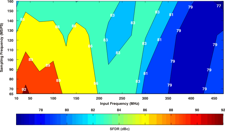
7.12.8 Contour
All graphs are at 25°C, AVDD = 1.8 V, DRVDD = 1.8 V, maximum rated sampling frequency, sine wave input clock. 1.5-VPP differential clock amplitude, 50% clock duty cycle, –1 dBFS differential analog input, High-Performance Mode disabled, 0-dB gain, DDR LVDS output interface, and 32k point FFT, unless otherwise noted.
 Figure 7-129 Spurious-Free Dynamic Range (0-dB Gain)
 Figure 7-130 Spurious-Free Dynamic Range (6-dB Gain)
 Figure 7-131 ADS424x
Signal-to-Noise Ratio (0-dB Gain)
 Figure 7-132 ADS424x
Signal-to-Noise Ratio (6-dB Gain)
 Figure 7-133 ADS422x
Signal-to-Noise Ratio (0-dB Gain)
 Figure 7-134 ADS422x
Signal-to-Noise Ratio (6-dB Gain)