JAJSR90A September 2023 – July 2024 LMQ64480-Q1 , LMQ644A0-Q1 , LMQ644A2-Q1
PRODUCTION DATA
- 1
- 1 特長
- 2 アプリケーション
- 3 概要
- 4 Device Comparison Table
- 5 Pin Configuration and Functions
- 6 Specifications
-
7 Detailed Description
- 7.1 Overview
- 7.2 Functional Block Diagram
- 7.3
Feature Description
- 7.3.1 Input Voltage Range (VIN)
- 7.3.2 Enable EN Pin and Use as VIN UVLO
- 7.3.3 Output Voltage Selection and Soft Start
- 7.3.4 SYNC Allows Clock Synchronization and Mode Selection
- 7.3.5 Clock Locking
- 7.3.6 Adjustable Switching Frequency
- 7.3.7 Power-Good Output Voltage Monitoring
- 7.3.8 Internal LDO, VCC UVLO, and BIAS Input
- 7.3.9 Bootstrap Voltage and VCBOOT-UVLO (CB1 and CB2 Pin)
- 7.3.10 CONFIG Device Configuration Pin
- 7.3.11 Spread Spectrum
- 7.3.12 Soft Start and Recovery From Dropout
- 7.3.13 Overcurrent and Short-Circuit Protection
- 7.3.14 Hiccup
- 7.3.15 Thermal Shutdown
- 7.4 Device Functional Modes
-
8 Application and Implementation
- 8.1 Application Information
- 8.2
Typical Application
- 8.2.1 Design Requirements
- 8.2.2
Detailed Design Procedure
- 8.2.2.1 Choosing the Switching Frequency
- 8.2.2.2 Setting the Output Voltage
- 8.2.2.3 Inductor Selection
- 8.2.2.4 Output Capacitor Selection
- 8.2.2.5 Input Capacitor Selection
- 8.2.2.6 BOOT Capacitor
- 8.2.2.7 VCC
- 8.2.2.8 CFF and RFF Selection
- 8.2.2.9 SYNCHRONIZATION AND MODE
- 8.2.2.10 External UVLO
- 8.2.2.11 Typical Thermal Performance
- 8.2.3 Application Curves
- 8.3 Power Supply Recommendations
- 8.4 Layout
- 9 Device and Documentation Support
- 10Revision History
- 11Mechanical, Packaging, and Orderable Information
7.3.13 Overcurrent and Short-Circuit Protection
The LMQ644xx is protected from overcurrent conditions by cycle-by-cycle current limiting on both the high-side and the low-side MOSFETs.
High-side MOSFET overcurrent protection is implemented by the nature of the peak current mode control. The HS switch current is sensed when the HS is turned on after a short blanking time. The HS switch current is compared to the output of the voltage regulation loop minus slope compensation, every switching cycle. Because the voltage loop has a maximum value and slope compensation increases with duty cycle, the HS current limit decreases with increased duty cycle such that the HS current limit is reduced by 35% for high output to input voltage duty ratios. See Figure 7-14.
 Figure 7-14 Maximum Current Allowed
Through the HS FET - Function of Duty Cycle for LMQ644xx
Figure 7-14 Maximum Current Allowed
Through the HS FET - Function of Duty Cycle for LMQ644xxWhen the LS switch is turned on, the current going through the LS switch is also sensed and monitored. Like the high-side device, the low-side device turn-off is commanded by the voltage control loop. For a low-side device, turn-off is prevented if current exceeds this value, even if the oscillator normally starts a new switching cycle. See Section 7.4.3.4. Also like the high-side device, there is a limit on how high the turn-off current is allowed to be. This is called the low-side current limit; see the Electrical Characteristics for values. If the LS current limit is exceeded, the LS MOSFET stays on and the HS switch is not turned on. The LS switch is turned off after the LS current falls below its limit. The HS switch is turned on again as long as at least one clock period has passed since the last time the HS device has turned on.
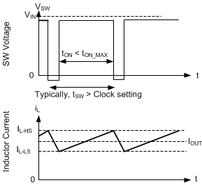
 Figure 7-15 Current Limit Waveforms
The net effect of the operation of high-side and low-side current limit is that the IC operates in hysteretic control. Because the current waveform assumes values between IL-HS and IL-LS, output current is close to the average of these two values unless duty cycle is very high. After operating in current limit, hysteretic control is used and current does not increase as output voltage approaches zero.
If duty cycle is very high, current ripple must be very low to prevent instability; see Section 8.2.2.3. Because current ripple is low, the part is able to deliver full current unless dropout across device is less than 0.5V. The current delivered is very close to IL-LS.
If overloaded, after the overload is removed, the device recovers as though in soft start; see Section 7.3.12. Note that hiccup can be triggered if output voltage drops below approximately 0.4 times the intended output voltage.