JAJSR90A September 2023 – July 2024 LMQ64480-Q1 , LMQ644A0-Q1 , LMQ644A2-Q1
PRODUCTION DATA
- 1
- 1 特長
- 2 アプリケーション
- 3 概要
- 4 Device Comparison Table
- 5 Pin Configuration and Functions
- 6 Specifications
-
7 Detailed Description
- 7.1 Overview
- 7.2 Functional Block Diagram
- 7.3
Feature Description
- 7.3.1 Input Voltage Range (VIN)
- 7.3.2 Enable EN Pin and Use as VIN UVLO
- 7.3.3 Output Voltage Selection and Soft Start
- 7.3.4 SYNC Allows Clock Synchronization and Mode Selection
- 7.3.5 Clock Locking
- 7.3.6 Adjustable Switching Frequency
- 7.3.7 Power-Good Output Voltage Monitoring
- 7.3.8 Internal LDO, VCC UVLO, and BIAS Input
- 7.3.9 Bootstrap Voltage and VCBOOT-UVLO (CB1 and CB2 Pin)
- 7.3.10 CONFIG Device Configuration Pin
- 7.3.11 Spread Spectrum
- 7.3.12 Soft Start and Recovery From Dropout
- 7.3.13 Overcurrent and Short-Circuit Protection
- 7.3.14 Hiccup
- 7.3.15 Thermal Shutdown
- 7.4 Device Functional Modes
-
8 Application and Implementation
- 8.1 Application Information
- 8.2
Typical Application
- 8.2.1 Design Requirements
- 8.2.2
Detailed Design Procedure
- 8.2.2.1 Choosing the Switching Frequency
- 8.2.2.2 Setting the Output Voltage
- 8.2.2.3 Inductor Selection
- 8.2.2.4 Output Capacitor Selection
- 8.2.2.5 Input Capacitor Selection
- 8.2.2.6 BOOT Capacitor
- 8.2.2.7 VCC
- 8.2.2.8 CFF and RFF Selection
- 8.2.2.9 SYNCHRONIZATION AND MODE
- 8.2.2.10 External UVLO
- 8.2.2.11 Typical Thermal Performance
- 8.2.3 Application Curves
- 8.3 Power Supply Recommendations
- 8.4 Layout
- 9 Device and Documentation Support
- 10Revision History
- 11Mechanical, Packaging, and Orderable Information
7.4.3.1 Peak Current Mode Operation
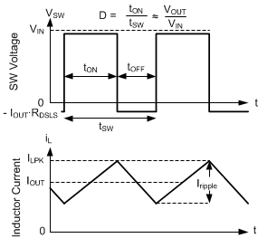
The following operating description of the LMQ644xx refers to Functional Block Diagram and the waveforms in Figure 7-18. Both supply a regulated output voltage by turning on the internal high-side (HS) and low-side (LS) NMOS switches with varying duty cycle (D). During the HS switch on-time, the SW terminal voltage, VSW, swings up to approximately VIN, and the inductor current, iL, increases with a linear slope. The HS switch is turned off by the control logic. During the HS switch off-time, tOFF, the LS switch is turned on. Inductor current discharges through the LS switch, forcing VSW to swing below ground by the voltage drop across the LS switch. The regulator loop adjusts the duty cycle to maintain a constant output voltage. D is defined by the on-time of the HS switch over the switching period: D = TON / (TON + TOFF).
In an ideal buck converter where losses are ignored, D is proportional to the output voltage and inversely proportional to the input voltage: D = VOUT / VIN.
 Figure 7-18 SW Voltage and Inductor Current Waveforms in Continuous Conduction Mode (CCM)
To get accurate DC load regulation, a voltage feedback loop is used. Peak and valley inductor currents are sensed for peak current mode control and current protection. The regulator operates with continuous conduction mode with constant switching frequency when load level is above one half of the minimum peak inductor current. The internally-compensated regulation network achieves fast and stable operation with small external components and low-ESR capacitors.