JAJSRY1G June   1998  – July 2024 SN74AHC367

PRODUCTION DATA  

  1.   1
  2. 特長
  3. アプリケーション
  4. 概要
  5. Pin Configurations and Functions
  6. Specifications
    1. 5.1 Absolute Maximum Ratings
    2. 5.2 ESD Ratings
    3. 5.3 Recommended Operating Conditions
    4. 5.4 Thermal Information
    5. 5.5 Electrical Characteristics
    6. 5.6 Switching Characteristics, VCC = 3.3 V ± 0.3 V
    7. 5.7 Switching Characteristics, VCC = 5 V ± 0.5 V
    8. 5.8 Noise Characteristics
    9. 5.9 Operating Characteristics
  7. Parameter Measurement Information
  8. Detailed Description
    1. 7.1 Overview
    2. 7.2 Functional Block Diagram
    3. 7.3 Device Functional Modes
  9. Application and Implementation
    1. 8.1 Application Information
    2. 8.2 Typical Application
    3. 8.3 Power Supply Recommendations
    4. 8.4 Layout
      1. 8.4.1 Layout Guidelines
      2. 8.4.2 Layout Example
  10. Device and Documentation Support
    1. 9.1 Documentation Support (Analog)
      1. 9.1.1 Related Documentation
    2. 9.2 ドキュメントの更新通知を受け取る方法
    3. 9.3 サポート・リソース
    4. 9.4 Trademarks
    5. 9.5 静電気放電に関する注意事項
    6. 9.6 用語集
  11. 10Revision History
  12. 11Mechanical, Packaging, and Orderable Information

Pin Configurations and Functions

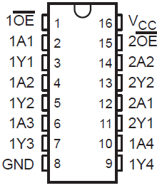
SN74AHC367 D, DB, DGV, N, or PW
                        Package (Top View)Figure 4-1 D, DB, DGV, N, or PW Package (Top View)
Table 4-1 Pin Functions
PIN TYPE DESCRIPTION
NO. NAME
1 1 OE I Output Enable 1
2 1A1 I 1A1 Input
3 1Y1 O 1Y1 Output
4 1A2 I 1A2 Input
5 1Y2 O 1Y2 Output
6 1A3 I 1A3 Input
7 1Y3 O 1Y3 Output
8 GND Ground Pin
9 1Y4 O 1Y4 Output
10 1A4 I 1A4 Input
11 2Y1 O 2Y1 Output
12 2A1 I 2A1 Input
13 2Y2 O 2Y2 Output
14 2A2 I 2A2 Input
15 2 OE I Output Enable 2
16 VCC Power Pin