JAJSSS9 July 2024 TLVM14404 , TLVM14406
PRODUCTION DATA
- 1
- 1 特長
- 2 アプリケーション
- 3 概要
- 4 Device Comparison Table
- 5 Pin Configuration and Functions
- 6 Specifications
-
7 Detailed Description
- 7.1 Overview
- 7.2 Functional Block Diagram
- 7.3
Feature Description
- 7.3.1 Input Voltage Range (VIN1, VIN2)
- 7.3.2 Enable EN Pin and Use as VIN UVLO
- 7.3.3 CONFIG Device Configuration Pin
- 7.3.4 Adjustable Switching Frequency
- 7.3.5 Adjustable Output Voltage (FB)
- 7.3.6 Input Capacitors
- 7.3.7 Output Capacitors
- 7.3.8 Power-Good Output Voltage Monitoring
- 7.3.9 Bias Supply Regulator (VCC, VOSNS)
- 7.3.10 Overcurrent Protection (OCP)
- 7.3.11 Thermal Shutdown
- 7.4 Device Functional Modes
-
8 Applications and Implementation
- 8.1 Application Information
- 8.2 Typical Applications
- 8.3 Power Supply Recommendations
- 8.4 Layout
- 9 Device and Documentation Support
- 10Revision History
- 11Mechanical, Packaging, and Orderable Information
7.3.2 Enable EN Pin and Use as VIN UVLO
Apply a voltage less than 0.25V to the EN1 pin to put the TLVM1440x into shutdown mode. In shutdown mode, the quiescent current drops to 0.5µA (typical). Above this voltage but below the lower EN threshold, VCC is active but switching on SW1 and SW2 remains inactive. After EN1 is above VEN, the SW1 becomes active. EN2 controls switching on the second output SW2. In dual output configuration EN2 can be used to independently turn off the second output voltage, but does not control when the device enters shutdown mode. In single output configuration EN1 must not be used to disable the secondary device for phase shedding and must be tied to EN2. The very high efficiency of the device in PFM operation eliminates the need to phase shed in most designs as phase of the secondaries is controlled even under PFM operation.
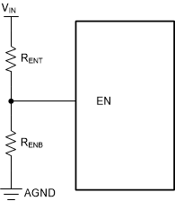
The EN terminals can not be left floating. The simplest method to enable the operation is to connect the EN pins to VIN. This action allows the self-start-up of the device when VIN drives the internal VCC above the UVLO level. However, many applications benefit from employing an enable divider string, which establishes a precision input undervoltage lockout (UVLO). The precision UVLO can be used for the following:
- Sequencing
- Preventing the device from retriggering when used with long input cables
- Reducing the occurrence of deep discharge of a battery power source
 Figure 7-2 VIN UVLO Using the EN Pin
Resistor values can be calculated using the following equations.
where
- VON = VIN turn-on voltage
- VOFF = VIN turn-off voltage