JAJSSZ9I September   2008  – May 2024 TL720M05-Q1

PRODMIX  

  1.   1
  2. 特長
  3. アプリケーション
  4. 概要
  5. Pin Configuration and Functions
  6. Specifications
    1. 5.1 Absolute Maximum Ratings
    2. 5.2 ESD Ratings
    3. 5.3 Recommended Operating Conditions
    4. 5.4 Thermal Information
    5. 5.5 Electrical Characteristics
    6. 5.6 Typical Characteristics
  7. Parameter Measurement Information
  8. Detailed Description
    1. 7.1 Overview
    2. 7.2 Functional Block Diagrams
    3. 7.3 Feature Description
      1. 7.3.1 Undervoltage Lockout
      2. 7.3.2 Thermal Shutdown
      3. 7.3.3 Current Limit
    4. 7.4 Device Functional Modes
      1. 7.4.1 Normal Operation
      2. 7.4.2 Dropout Operation
      3. 7.4.3 Disabled
  9. Application and Implementation
    1. 8.1 Application Information
      1. 8.1.1 Input and Output Capacitor Selection
        1. 8.1.1.1 Legacy Chip Capacitor Selection
        2. 8.1.1.2 New Chip Output Capacitor
        3. 8.1.1.3 New Chip Input Capacitor
      2. 8.1.2 Dropout Voltage
      3. 8.1.3 Reverse Current
      4. 8.1.4 Power Dissipation (PD)
        1. 8.1.4.1 Thermal Performance Versus Copper Area
        2. 8.1.4.2 Power Dissipation Versus Ambient Temperature
      5. 8.1.5 Estimating Junction Temperature
    2. 8.2 Typical Application
      1. 8.2.1 Design Requirements
      2. 8.2.2 Detailed Design Procedure
        1. 8.2.2.1 Input Capacitor
        2. 8.2.2.2 Output Capacitor
      3. 8.2.3 Application Curves
    3. 8.3 Power Supply Recommendations
    4. 8.4 Layout
      1. 8.4.1 Layout Guidelines
      2. 8.4.2 Layout Examples
  10. Device and Documentation Support
    1. 9.1 Device Support
      1. 9.1.1 Evaluation Module
      2. 9.1.2 Device Nomenclature
      3. 9.1.3 Development Support
    2. 9.2 Documentation Support
      1. 9.2.1 Related Documentation
    3. 9.3 ドキュメントの更新通知を受け取る方法
    4. 9.4 サポート・リソース
    5. 9.5 Trademarks
    6. 9.6 静電気放電に関する注意事項
    7. 9.7 用語集
  11. 10Revision History
  12. 11Mechanical, Packaging, and Orderable Information

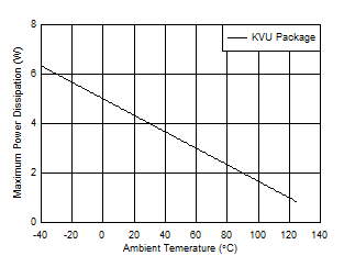
Power Dissipation Versus Ambient Temperature

Figure 8-4 is based off of a JESD51-7 4-layer, high-K board. Estimate the allowable power dissipation with the following equation. Improve thermal dissipation in the JEDEC high-K layout by adding top layer copper and increasing the number of thermal vias. See the An empirical analysis of the impact of board layout on LDO thermal performance application note. If a good thermal layout is used, the allowable thermal dissipation is improved by up to 50%.

Equation 4. TL720M05-Q1
TL720M05-Q1 TL720M05-Q1 Allowable Power
                    Dissipation Figure 8-4 TL720M05-Q1 Allowable Power Dissipation