JAJST23 June 2024 BQ41Z50
ADVANCE INFORMATION
- 1
- 1 特長
- 2 アプリケーション
- 3 概要
- 4 概要 (続き)
- 5 Pin Configuration and Functions
-
6 Specifications
- 6.1 Absolute Maximum Ratings
- 6.2 ESD Ratings
- 6.3 Recommended Operating Conditions
- 6.4 Thermal Information
- 6.5 Supply Current
- 6.6 Power Supply Control
- 6.7 Current Wake Detector
- 6.8 VC0, VC1, VC2, VC3, VC4, PACK
- 6.9 SMBD, SMBC
- 6.10 PRES/SHUTDN, DISP
- 6.11 ALERT
- 6.12 Coulomb Counter Digital Filter (CC1)
- 6.13 ADC Digital Filter
- 6.14 CHG, DSG High-side NFET Drivers
- 6.15 Precharge (PCHG) FET Drive
- 6.16 FUSE Drive
- 6.17 Internal Temperature Sensor
- 6.18 TS1, TS2, TS3, TS4
- 6.19 Flash Memory
- 6.20 GPIO1, GPIO2, GPIO3, GPIO4, GPIO5, GPIO6, GPIO7
- 6.21 Elliptical Curve Cryptography (ECC)
- 6.22 SMBus Interface Timing
- 6.23 Typical Characteristics
-
7 Detailed Description
- 7.1 Overview
- 7.2 Functional Block Diagram
- 7.3 Feature Description
- 7.4 Device Functional Modes
- 8 Applications and Implementation
- 9 Device and Documentation Support
- 10Revision History
- 11Mechanical, Packaging, and Orderable Information
8.4.1 Layout Guidelines
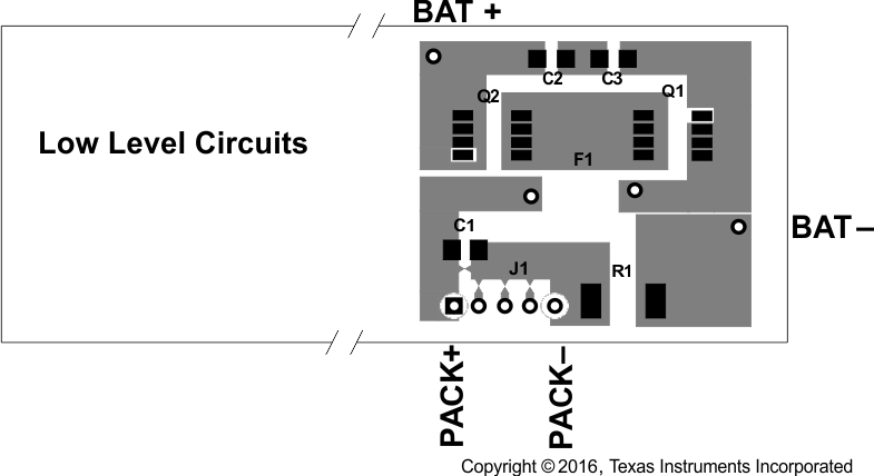
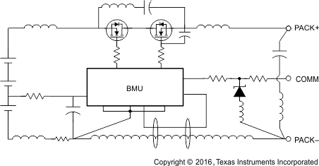
A battery fuel gauge circuit board is a challenging environment due to the fundamental incompatibility of high-current traces and ultra-low current semiconductor devices. The best way to protect against unwanted trace-to-trace coupling is with a component placement, such as that shown in Figure 8-16, where the high-current section is on the opposite side of the board from the electronic devices. Clearly this is not possible in many situations due to mechanical constraints. Still, every attempt should be made to route high-current traces away from signal traces, which enter the BQ41Z50 directly. IC references and registers can be disturbed and in rare cases damaged due to magnetic and capacitive coupling from the high-current path. Note that during surge current and ESD events, the high-current traces appear inductive and can couple unwanted noise into sensitive nodes of the gas gauge electronics, as illustrated in Figure 8-17.
 Figure 8-16 Separating High- and Low-Current Sections Provides an Advantage in Noise Immunity
 Figure 8-17 Avoid Close Spacing Between High-Current and Low-Level Signal Lines
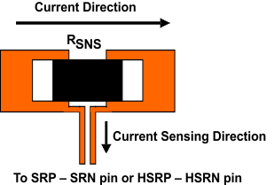
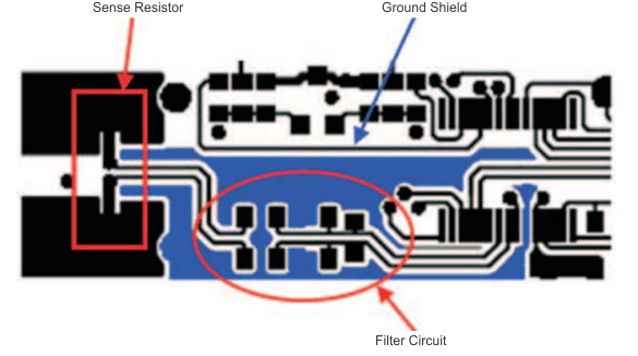
Kelvin voltage sensing is extremely important in order to accurately measure current and top and bottom cell voltages. Place all filter components as close as possible to the device. Route the traces from the sense resistor in parallel to the filter circuit. Adding a ground plane around the filter network can add additional noise immunity. Figure 8-18 and Figure 8-19 demonstrates correct kelvin current sensing.
 Figure 8-18 Sensing Resistor PCB Layout
 Figure 8-19 Sense Resistor, Ground Shield, and Filter Circuit Layout
Some suggestions to improve the system level resiliancy to ESD were tested and improved the performance significantly:
Add ground planes—Ground planes are used to add distributed capacitance to the layout itself, this reduces the voltage seen on the pins of the IC. For multilayer PCBs, separate the signal layers with a ground plane. Add more layers to improve the ESD system level performance.
Keep the VCC cap populated and as close as possible to the gauge IC.