JAJSTU7H August 2007 – July 2024 CDCE937 , CDCEL937
PRODUCTION DATA
- 1
- 1 特長
- 2 アプリケーション
- 3 概要
- 4 Pin Configuration and Functions
- 5 Specifications
- 6 Parameter Measurement Information
- 7 Detailed Description
- 8 Register Maps
- 9 Application and Implementation
- 10Power Supply Recommendations
- 11Layout
- 12Device and Documentation Support
- 13Revision History
- 14Mechanical, Packaging, and Orderable Information
9.2.2.2 PLL Frequency Planning
At a given input frequency (ƒIN), the output frequency (ƒOUT) of the CDCEx913 are calculated with Equation 1.
Equation 1. 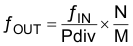
where
- M (1 to 511) and N (1 to 4095) are the multiplier/divide values of the PLL
- Pdiv (1 to 127) is the output divider
The target VCO frequency (ƒVCO) of each PLL is calculated with Equation 2.
Equation 2. 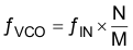
The PLL internally operates as fractional divider and needs the following multiplier/divider settings:
- N
- P = 4 – int(log2N/M; if P < 0 then P = 0
- Q = int(N'/M)
- R = N′ – M × Q
where
N′ = N × 2P
N ≥ M;
80 MHz ≤ ƒVCO ≤ 230 MHz
16 ≤ Q ≤ 63
0 ≤ P ≤ 4
0 ≤ R ≤ 51
| Example: | |||
| for ƒIN = 27 MHz; M = 1; N = 4; Pdiv = 2 | for ƒIN = 27 MHz; M = 2; N = 11; Pdiv = 2 | ||
| → | fOUT = 54 MHz | → | fOUT = 74.25 MHz |
| → | fVCO = 108 MHz | → | fVCO = 148.50 MHz |
| → | P = 4 – int(log24) = 4 – 2 = 2 | → | P = 4 – int(log25.5) = 4 – 2 = 2 |
| → | N' = 4 × 22 = 16 | → | N' = 11 × 22 = 44 |
| → | Q = int(16) = 16 | → | Q = int(22) = 22 |
| → | R = 16 – 16 = 0 | → | R = 44 – 44 = 0 |
The values for P, Q, R, and N’ are automatically calculated when using TI Pro-Clock™ software.