JAJSUC2B December   2015  – April 2024 LDC0851

PRODUCTION DATA  

  1.   1
  2. 特長
  3. アプリケーション
  4. 概要
  5. Pin Configuration and Functions
  6. Specifications
    1. 5.1 Absolute Maximum Ratings
    2. 5.2 ESD Ratings
    3. 5.3 Recommended Operating Conditions
    4. 5.4 Thermal Information
    5. 5.5 Electrical Characteristics
    6. 5.6 Interface Voltage Levels
    7. 5.7 Timing Requirements
    8. 5.8 Typical Characteristics
  7. Detailed Description
    1. 6.1 Overview
    2. 6.2 Functional Block Diagram
    3. 6.3 Feature Description
      1. 6.3.1 Basic Operation Mode
      2. 6.3.2 Threshold Adjust Mode
      3. 6.3.3 Setting the Threshold Adjust Values
      4. 6.3.4 Hysteresis
      5. 6.3.5 Conversion Time
      6. 6.3.6 Power-Up Conditions
    4. 6.4 Device Functional Modes
      1. 6.4.1 Shutdown Mode
      2. 6.4.2 Active Mode
  8. Application and Implementation
    1. 7.1 Application Information
      1. 7.1.1 Sensor Design
        1. 7.1.1.1 Sensor Frequency
        2. 7.1.1.2 Sensor Design Procedure
    2. 7.2 Typical Application
      1. 7.2.1 Event Counting
        1. 7.2.1.1 Design Requirements
        2. 7.2.1.2 Detailed Design Procedure
        3. 7.2.1.3 Application Curves
      2. 7.2.2 Coarse Position Sensing
        1. 7.2.2.1 Design Requirements
        2. 7.2.2.2 Detailed Design Procedure
        3. 7.2.2.3 Application Curves
      3. 7.2.3 Low Power Operation
        1. 7.2.3.1 Design Requirements
        2. 7.2.3.2 Detailed Design Procedure
        3. 7.2.3.3 Application Curves
    3. 7.3 Power Supply Recommendations
    4. 7.4 Layout
      1. 7.4.1 Layout Guidelines
      2. 7.4.2 Layout Example
        1. 7.4.2.1 Side by Side Coils
        2. 7.4.2.2 Stacked Coils
  9. Device and Documentation Support
    1. 8.1 Device Support
      1. 8.1.1 Development Support
    2. 8.2 Documentation Support
      1. 8.2.1 Related Documentation
    3. 8.3 サポート・リソース
    4. 8.4 Trademarks
    5. 8.5 静電気放電に関する注意事項
    6. 8.6 用語集
  10. Revision History
  11. 10Mechanical, Packaging, and Orderable Information

Pin Configuration and Functions

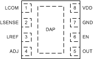
LDC0851 DSG Package8-Pin WSON with DAPTop View Figure 4-1 DSG Package8-Pin WSON with DAPTop View
Table 4-1 Pin Functions
PIN TYPE(1) DESCRIPTION
NAME NO.
LCOM 1 A Common coil input
LSENSE 2 A Sense coil input
LREF 3 A Reference coil input
ADJ 4 A Threshold adjust pin
OUT 5 O Switch output
EN 6 I Enable input
GND 7 G Ground
VDD 8 P Power Supply
DAP DAP G Connect to Ground for improved thermal performance(2)
I = Input, O = Output, P = Power, A = Analog, G = Ground
There is an internal electrical connection between the exposed Die Attach Pad (DAP) and the GND pin of the device. Although the DAP can be left floating, for best performance the DAP should be connected to the same potential as the device's GND pin. Do not use the DAP as the primary ground for the device. The device GND pin must always be connected to ground.