JAJSUP6B November   2013  – May 2024 TPS61162A , TPS61163A

PRODUCTION DATA  

  1.   1
  2. 特長
  3. アプリケーション
  4. 概要
  5. Pin Configuration and Functions
    1.     Pin Functions
  6. Specifications
    1. 5.1 Absolute Maximum Ratings
    2. 5.2 ESD Ratings
    3. 5.3 Recommended Operating Conditions
    4. 5.4 Thermal Information
    5. 5.5 Electrical Characteristics
    6. 5.6 EasyScale Timing Requirements
    7. 5.7 Typical Characteristics
  7. Detailed Description
    1. 6.1 Overview
    2. 6.2 Functional Block Diagram
    3. 6.3 Feature Description
      1. 6.3.1  Boost Converter
      2. 6.3.2  IFBx Pin Unused
      3. 6.3.3  Enable and Start-up
      4. 6.3.4  Soft Start
      5. 6.3.5  Full-Scale Current Program
      6. 6.3.6  Brightness Control
      7. 6.3.7  Undervoltage Lockout
      8. 6.3.8  Overvoltage Protection
      9. 6.3.9  Overcurrent Protection
      10. 6.3.10 Thermal Shutdown
    4. 6.4 Device Functional Modes
      1. 6.4.1 One-Wire Digital Interface (EasyScale Interface)
      2. 6.4.2 PWM Control Interface
    5. 6.5 Programming
      1. 6.5.1 EasyScale Programming
  8. Application and Implementation
    1. 7.1 Application Information
    2. 7.2 Typical Application
      1. 7.2.1 Design Requirements
      2. 7.2.2 Detailed Design Procedure
        1. 7.2.2.1 Inductor Selection
        2. 7.2.2.2 Schottky Diode Selection
        3. 7.2.2.3 Compensation Capacitor Selection
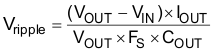
        4. 7.2.2.4 Output Capacitor Selection
      3. 7.2.3 Application Curves
      4. 7.2.4 Additional Application Circuits
    3. 7.3 Power Supply Recommendations
    4. 7.4 Layout
      1. 7.4.1 Layout Guidelines
      2. 7.4.2 Layout Example
  9. Device and Documentation Support
    1. 8.1 Device Support
    2. 8.2 Related Links
    3. 8.3 Community Resources
    4. 8.4 Trademarks
  10. Revision History
  11. 10Mechanical, Packaging, and Orderable Information

Output Capacitor Selection

The output capacitor is mainly selected to meet the requirement for the output ripple and loop stability. A 1-µF to 2.2-µF capacitor is recommended for the loop stability consideration. This ripple voltage is related to the capacitor’s capacitance and its ESR. Due to its low ESR, Vripple_ESR could be neglected for ceramic capacitors. Assuming a capacitor with zero ESR, the output ripple can be calculated with Equation 7.

Equation 7. TPS61162A TPS61163A

where

  • Vripple = peak-to-peak output ripple.

The additional part of ripple caused by the ESR is calculated using Vripple_ESR = IOUT x RESR and can be ignored for ceramic capacitors.

Note that capacitor degradation increases the ripple much. Select the capacitor with 50-V rated voltage to reduce the degradation at the output voltage. If the output ripple is too large, change a capacitor with less degradation effect or with higher rated voltage could be helpful.